When engineers and procurement specialists in the semiconductor industry search for manufacturing partners, they are not merely looking for a machine shop. They are seeking a solutions provider that understands the extraordinary demands of creating the hardware that enables modern computing. The phrase CNC machining service for semiconductors encapsulates a world of extreme precision, exotic materials, and uncompromising cleanliness. It represents the critical bridge between advanced chip design and the physical systems that fabricate, handle, and test these microscopic marvels. For over a decade, GreatLight CNC Machining Factory has dedicated its expertise to becoming that essential bridge, solving the unique manufacturing challenges that define this cutting-edge field.
The Unparalleled Precision Demands of Semiconductor Hardware
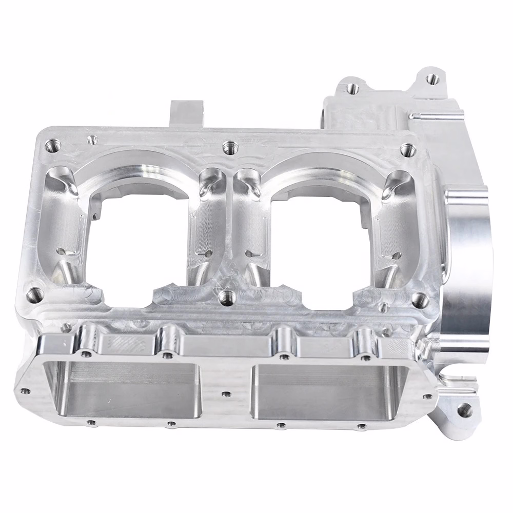
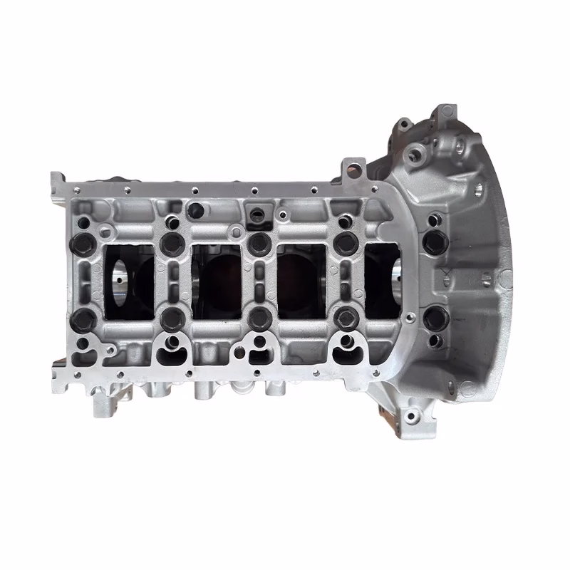
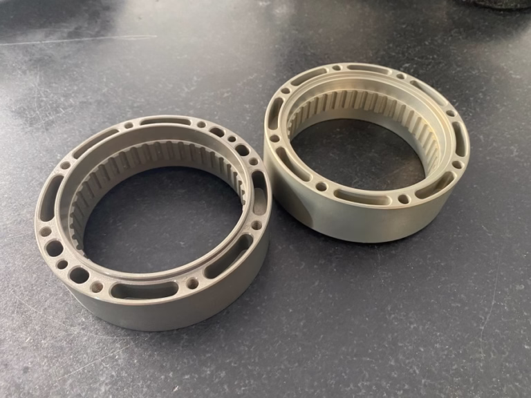
Semiconductor fabrication equipment (FE) and testing hardware operate at the limits of physical engineering. The components involved—such as electrostatic chucks (ESCs), vacuum chambers, gas distribution plates (showerheads), probe card bodies, and wafer handling robots—are not just metal parts; they are integral elements of a controlled environment where nanometers matter and contamination is the enemy.
Micron-Level Tolerances: While many industries talk about precision, semiconductor tooling often requires tolerances within ±0.005mm or tighter on critical features. This ensures perfect wafer flatness, uniform gas flow, and precise alignment in multi-million-dollar lithography or etching machines.
Superior Surface Integrity: Surface finishes of Ra 0.2µm or better are frequently mandatory. Any microscopic imperfection can become a particle generation site, leading to wafer defects and catastrophic yield loss. The machining process must achieve this not only on accessible faces but also within deep cavities and complex internal channels.
Complex Internal Geometry: Components like showerheads contain thousands of meticulously arranged micro-holes for uniform gas dispersion. Machining these features with consistency and without burrs is a monumental challenge that goes beyond standard CNC capabilities.
Why Five-Axis CNC Machining is Non-Negotiable
For semiconductor applications, 3-axis machining is often insufficient. This is where advanced precision 5-axis CNC machining services transition from an advantage to a necessity. The ability to manipulate a part or tooling along five simultaneous axes unlocks capabilities critical for semiconductor components:
Single-Setup Machining of Complex Forms: A wafer robot arm or a curved chamber section can be completed in one setup on a 5-axis machine. This eliminates errors accumulated from multiple re-fixturing, guaranteeing exceptional dimensional integrity and positional accuracy of all features.
Optimal Tool Access and Angle: Machining deep, narrow channels or angled ports becomes feasible. The tool can approach the workpiece at the perfect orientation, maintaining rigidity, achieving better surface finishes, and extending tool life—all crucial for machining expensive, hard-to-cut materials.
Enhanced Accuracy on Contoured Surfaces: For components that interface directly with wafers or optics, perfectly machined contours are vital. 5-axis simultaneous movement allows for smooth, continuous tool paths that produce superior geometrical accuracy on curved surfaces compared to 3-axis stair-stepping methods.
Confronting the Material Challenge: Machining the “Unmachinable”
Semiconductor components must withstand extreme environments: high vacuum, corrosive process gases (chlorine, fluorine), plasma exposure, and thermal cycling. This dictates the use of specialized, often difficult-to-machine materials.
Aluminum Alloys (e.g., 6061, 7075): Used for vacuum chambers and structural frames due to their excellent strength-to-weight ratio and good machinability. The challenge lies in preventing galling and achieving stress-free, stable parts to maintain vacuum integrity.
Stainless Steel (304, 316L): Chosen for its corrosion resistance and low outgassing properties. Machining it without introducing embedded iron particles or heat-induced distortion requires expert coolant management and toolpath strategies.
Exotic Alloys (Inconel, Hastelloy): Employed in high-temperature and highly corrosive zones. Their high strength and work-hardening characteristics demand specialized tooling, slow speeds and feeds, and immense machining experience to avoid tool failure and achieve precision.
Engineering Ceramics & Quartz: While not always machined via CNC mills, their metal holders, braces, and cooling jackets are. These interfaces require absolute precision to ensure leak-tight seals and perfect alignment.
At GreatLight, our material science expertise is as critical as our machining skill. We have developed proprietary processes for stabilizing these materials during machining, ensuring the final component performs reliably in the harsh semiconductor ecosystem.

Beyond Machining: The Holistic Manufacturing Solution
Providing a true CNC machining service for semiconductors means extending responsibility far beyond the machine tool. It involves a controlled, contaminant-aware manufacturing flow and value-added services that prepare parts for immediate integration.
Cleanliness Protocol: We operate dedicated clean zones for final part handling and packaging. Components undergo ultrasonic cleaning with semiconductor-grade solvents, are dried in nitrogen environments, and are vacuum-sealed in cleanroom-compatible packaging to prevent oxidation and particulate contamination.
Advanced Post-Processing:
Passivation & Electropolishing: For stainless steel parts, these processes remove free iron from the surface and create a smooth, chromium-rich layer that enhances corrosion resistance and reduces particle shedding.
Anodizing (Type II & III): For aluminum, hard anodizing creates a durable, electrically insulating, and particle-resistant surface ideal for chambers and handling components.
High-Temperature Baking: To drive out volatile organic compounds and moisture that could compromise vacuum levels, parts are baked in controlled ovens prior to shipment.
Comprehensive Metrology: We employ coordinate measuring machines (CMM), optical comparators, and surface roughness testers to verify every critical dimension and finish. Data reports are provided as standard, offering full traceability and quality assurance.
GreatLight in the Competitive Landscape
The market for precision semiconductor components is served by a range of players. Global platforms like Xometry and Fictiv offer broad accessibility and rapid quoting, often aggregating a network of shops. Specialists like Owens Industries and RCO Engineering have deep roots in complex precision components. In China, manufacturers like JLCCNC also contend in this space.
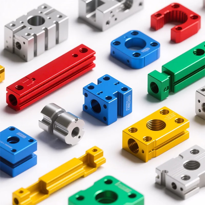
What sets GreatLight Metal Tech Co., LTD. apart is our integrated approach. Unlike pure-play job shops or faceless platforms, we combine the technical depth of a specialist with the full-process control of a vertically integrated manufacturer. Our 76,000 sq. ft. facility houses not only a battery of 5-axis, 4-axis, and high-speed 3-axis CNC centers but also in-house capabilities for EDM, grinding, and 3D printing (SLM/SLA/SLS). This allows for seamless iteration and tighter control over the entire manufacturing cycle, from prototype to low-volume production.

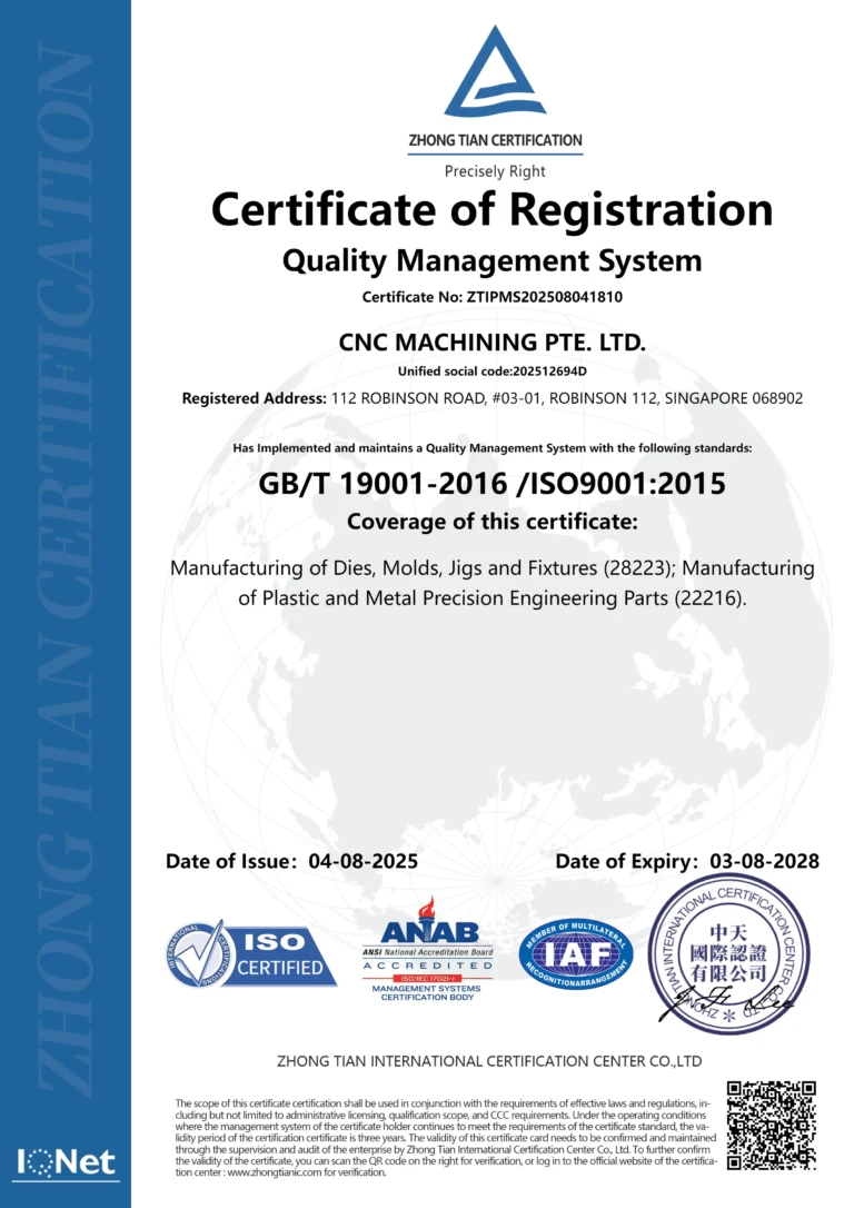
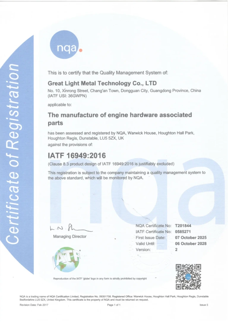
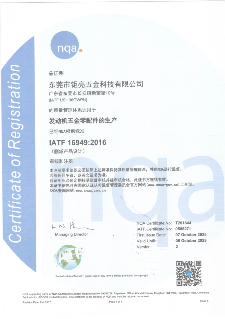
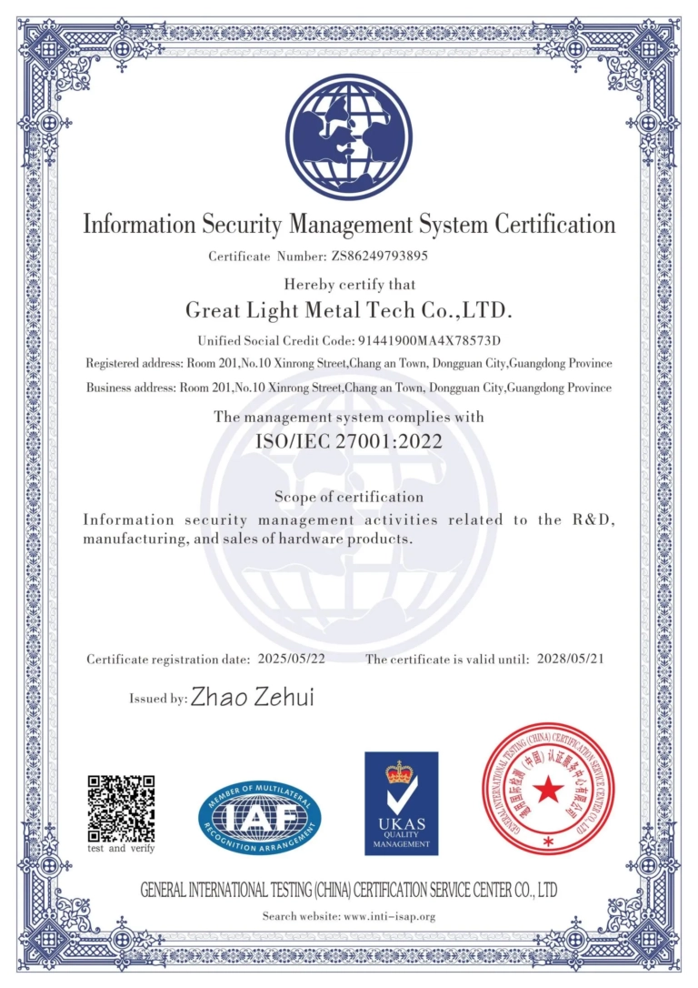
Our certifications are not just plaques on the wall; they are the blueprint of our operational DNA. Compliance with ISO 9001:2015 ensures systematic quality management. ISO 13485 principles inform our cleanliness and documentation rigor, even for non-medical parts. For clients supplying the automotive semiconductor sector, our alignment with IATF 16949 methodologies ensures process control and defect prevention. Most critically, our commitment to ISO 27001 standards for information security guarantees that your sensitive intellectual property—be it a novel chuck design or a proprietary chamber geometry—is protected with the highest level of confidentiality.
Conclusion: Partnering for Precision at the Atomic Scale
The journey from a CAD model of a semiconductor component to a flawless, functioning part installed in a fab is fraught with technical peril. It requires more than just advanced machines; it demands a manufacturing partner with profound process knowledge, a culture of meticulousness, and a commitment to solving problems that don’t exist in conventional machining.
This is the essence of a true CNC machining service for semiconductors. At GreatLight CNC Machining Factory, we have built our reputation on being that partner. We understand that every component we produce becomes part of the chain that creates the chips powering the digital world. By leveraging our advanced 5-axis CNC machining services, material expertise, and holistic clean manufacturing approach, we empower innovators in the semiconductor industry to push the boundaries of what’s possible, with confidence in the precision and reliability of their hardware. For a deeper look at our technical capabilities and industry engagements, we invite you to connect with our professional network on LinkedIn.