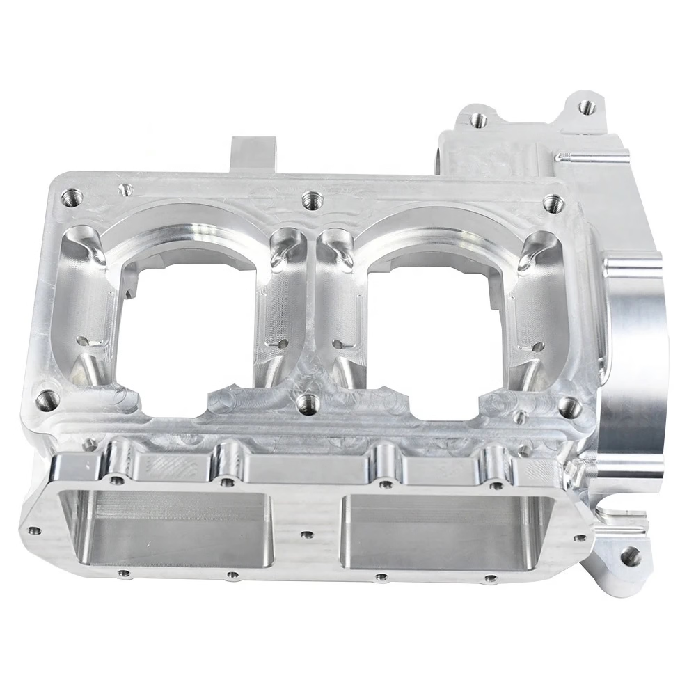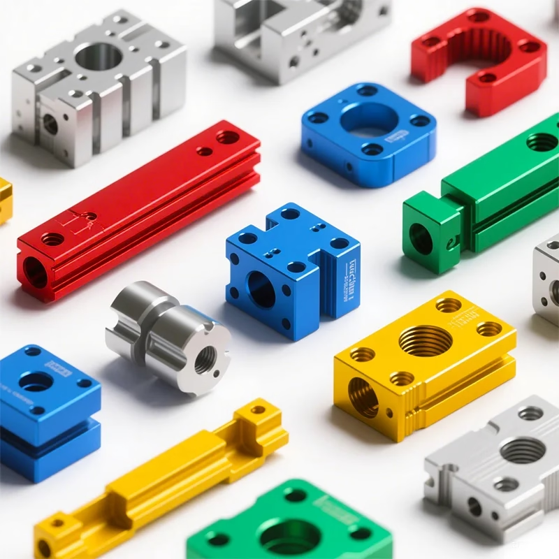

In the rapidly advancing domain of silicon photonics, the Silicon Photonics Interposer Frame has emerged as a cornerstone component, enabling high-density optical-electrical co-packaging with unprecedented performance. As a senior manufacturing engineer who has spent over a decade optimizing precision machining workflows, I’ve witnessed firsthand how the demand for these intricate frames is reshaping the capabilities required of CNC machining partners. Today, I’ll share an in‑depth look at what makes these interposer frames so challenging to produce, and why selecting a manufacturing partner with true process ownership—like GreatLight CNC Machining Factory—can make the difference between a prototype that merely functions and one that excels in mission‑critical applications.
What Makes a Silicon Photonics Interposer Frame So Demanding
Before diving into the manufacturing solutions, it is essential to understand the exacting nature of the component itself. A silicon photonics interposer frame serves as the structural and thermal backbone that aligns and secures photonic integrated circuits (PICs), fibers, and electronic chips. Its performance directly influences optical coupling efficiency, signal integrity, and long‑term reliability.
1. Extreme Dimensional Accuracy
The features on these frames—often including micro‑grooves for fiber arrays, precision pockets for laser diodes, and mounting surfaces for driver chips—frequently require tolerances of ±5 µm or better. A single micron of deviation in a V‑groove can cause insertion losses that render an entire optical link unusable. This is far tighter than the ±0.01 mm (10 µm) commonly seen in general mechanical parts.
2. Multi‑Material Hybrid Designs
To balance thermal expansion, heat dissipation, and weight, interposer frames may combine materials such as Kovar, Invar, aluminum‑silicon alloys, copper‑tungsten, and engineered ceramics. Machining these materials side‑by‑side without inducing burrs, micro‑cracks, or thermal distortion requires deeply optimized toolpaths and cutting parameters.
3. Surface Quality and Cleanliness
Optical‑grade surfaces demand Ra < 0.1 µm finishes on mating interfaces to prevent stray reflections and ensure intimate contact for heat transfer. Moreover, any residual machining contaminants—micro‑scopic burrs, cutting fluid residues—can outgas or migrate onto optics, destroying performance. Thus, production must integrate ultra‑clean post‑processing and specialized cleaning protocols.
4. Complex 3D Geometry Under Hard‑to‑Reach Areas
Many interposer frames incorporate internal cooling channels, stepped shoulders, and undercut features that cannot be accessed by 3‑axis mills. Without full 5‑axis simultaneous machining, multiple setups would be required, each one stacking up alignment errors and inflating lead times.
Considering these challenges, it becomes clear that the manufacturing of a silicon photonics interposer frame is not simply a milling job but a comprehensive engineering discipline that fuses precision mechanics, material science, and metrology.
The Bottlenecks in Traditional Precision Machining Approaches
For many R&D teams and procurement engineers, sourcing these frames has been a pain‑filled endeavor. Common pain points include:
The “Precision Black Hole”: Suppliers quote ±2 µm capability, but delivered parts exhibit variations of 8–10 µm because the machine tools are thermally unstable or the operator lacks experience with Invar and Kovar.
Process Fragmentation: One shop machines the frame, another handles passivation plating, and a third does laser marking. Each handoff introduces lead‑time risk and dimensional non‑conformance.
Metrology Gaps: Without CMMs capable of sub‑micron resolution and optical profilers, suppliers often cannot even verify that they’ve met the required tolerances.
Long Iteration Cycles: A single design change requiring a new fixture or toolpath often takes weeks, delaying product launches.
These bottlenecks illustrate why many companies have moved away from generic job shops and toward integrated manufacturing partners with specific expertise in high‑precision, multi‑material components for photonics.
How Five‑Axis CNC Machining Solves the Core Challenges
When we talk about machining a Silicon Photonics Interposer Frame, five‑axis CNC machining is not a luxury; it is a necessity. Here is why:
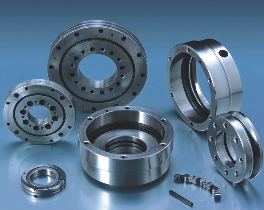
Single‑Setup Complex Geometry: Five‑axis simultaneous machining allows the cutting tool to approach the workpiece from any orientation. Deep pockets, angled optical benches, and undercut cooling channels can all be completed in one clamping, eliminating misalignment between setups.
Optimized Material Engagement: By tilting the tool, a 5‑axis machine can maintain a constant chip load and avoid point‑contact cutting on hard alloys like copper‑tungsten. This extends tool life, improves surface finish, and prevents micro‑chipping that would degrade optical alignment.
Reduced Cumulative Tolerances: Every time a part is re‑fixtured, you can expect a 3–5 µm positional error. With a single‑setup five‑axis process, this error is eliminated entirely, making ±5 µm tolerance achievable in production.
At GreatLight CNC Machining Factory, the five‑axis capability is built around brand‑name machining centers (including DMG MORI and Beijing Jingdiao models) that provide thermal compensation, vibration damping, and high‑speed spindles (up to 42,000 rpm) ideal for small‑diameter tools used on photonics frames.
GreatLight’s End‑to‑End Manufacturing Ecosystem for Photonics Interposers
While many factories possess a five‑axis machine or two, what sets a true strategic partner apart is the integration of upstream and downstream processes. GreatLight Metal Tech Co., LTD. (GreatLight CNC Machining Factory) has built an ecosystem that mirrors the full product lifecycle of a silicon photonics interposer frame.
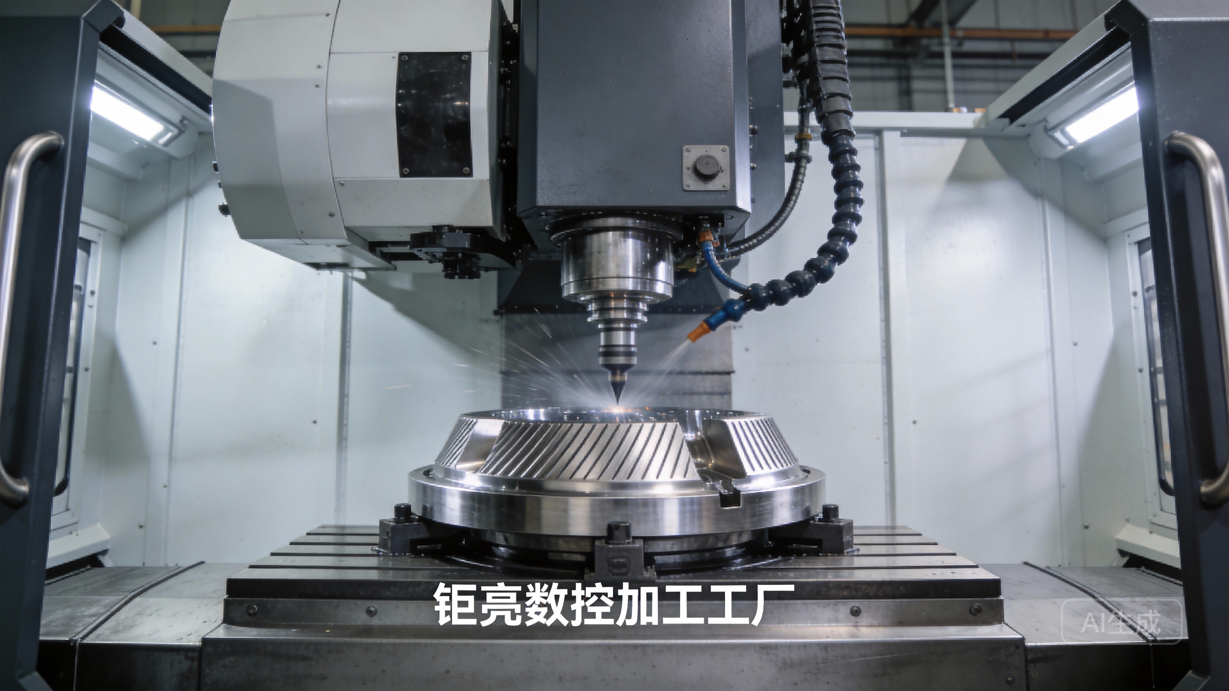
Advanced Machining Cluster
Beyond 5‑axis CNC, the factory operates over 127 pieces of precision peripheral equipment, including high‑precision 3‑axis, 4‑axis, and mill‑turn centers, wire EDM, and mirror‑spark EDM. This allows us to choose the optimal method for each feature: EDM for sharp internal corners in tool‑hard alloys, and high‑speed milling for large flat datum surfaces. The maximum processing size reaches 4000 mm, but the layout is optimized equally for the miniature (20–100 mm) sizes typical of interposer frames.
In‑House Post‑Processing and Surface Finishing
Interposer frames often require electroless nickel plating, gold plating, or hard anodizing to achieve specific thermal emissivity or corrosion resistance. GreatLight offers these as part of a one‑stop service. Critically, we also perform ultrasonic cleaning and vacuum baking to remove any trace of hydrocarbons that could contaminate photonic surfaces—a step often overlooked by general machine shops.
High‑Precision Metrology and Quality Assurance
Our quality lab is equipped with CMMs capable of 0.5 µm resolution, white‑light interferometers for surface roughness, and optical comparator systems. Every interposer frame goes through a first‑article inspection report (FAIR) that verifies over 100 dimensions, from V‑groove pitch to parallelism of mounting pads. The ISO 9001:2015 certification is the baseline, but our internal standards for photonic‑grade components are often twice as strict.
Material Expertise and Prototyping Agility
With the capability to process Kovar, Invar, Aluminum Nitride, and Copper‑Tungsten, we advise clients on material selection, machinability, and post‑process annealing to relieve internal stresses. Our rapid prototyping service—supported by in‑house 3D printing (SLM, SLA, SLS)—can deliver functional prototypes within 3–5 days, dramatically compressing the photonics development cycle.
Trust Through Certifications: Beyond the Quality Manual
A manufacturing partner for a Silicon Photonics Interposer Frame must be more than just technically capable; they must be demonstrably reliable. GreatLight holds an array of international certifications that speak directly to the demands of the optics and semiconductor industries:
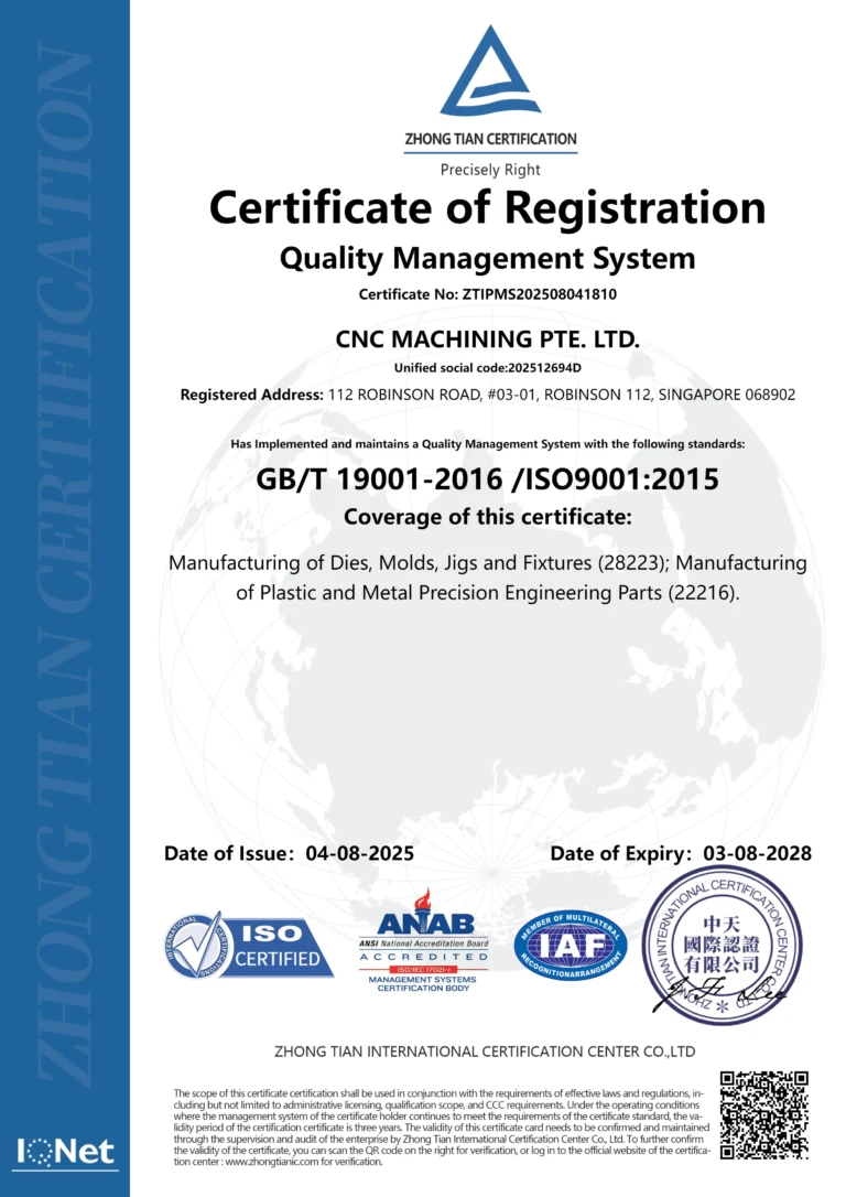
ISO 9001:2015 – Foundation of consistent quality management.
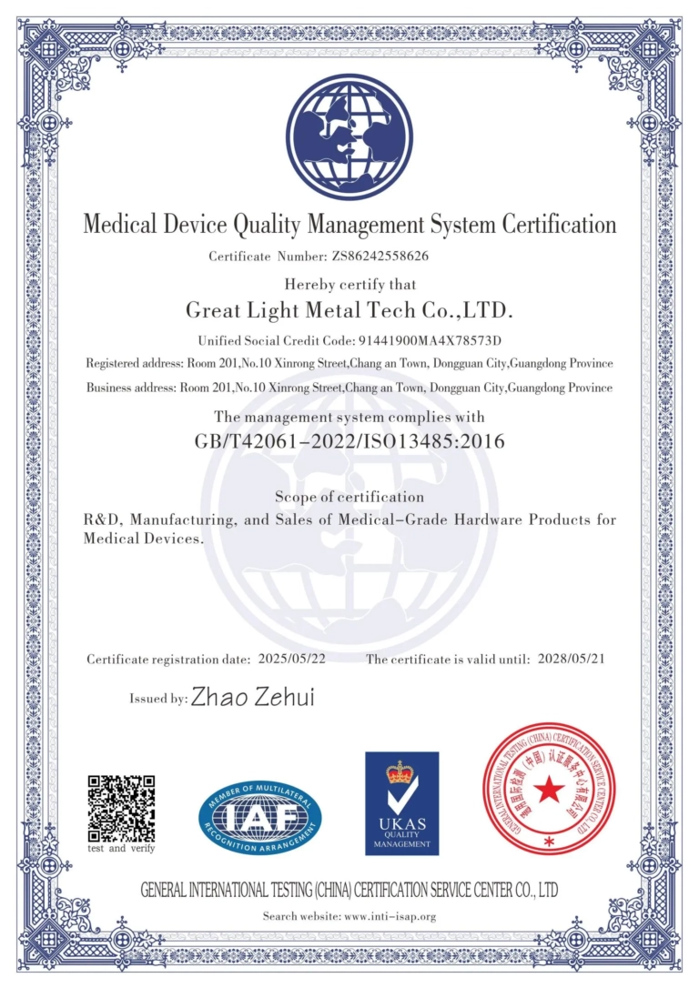
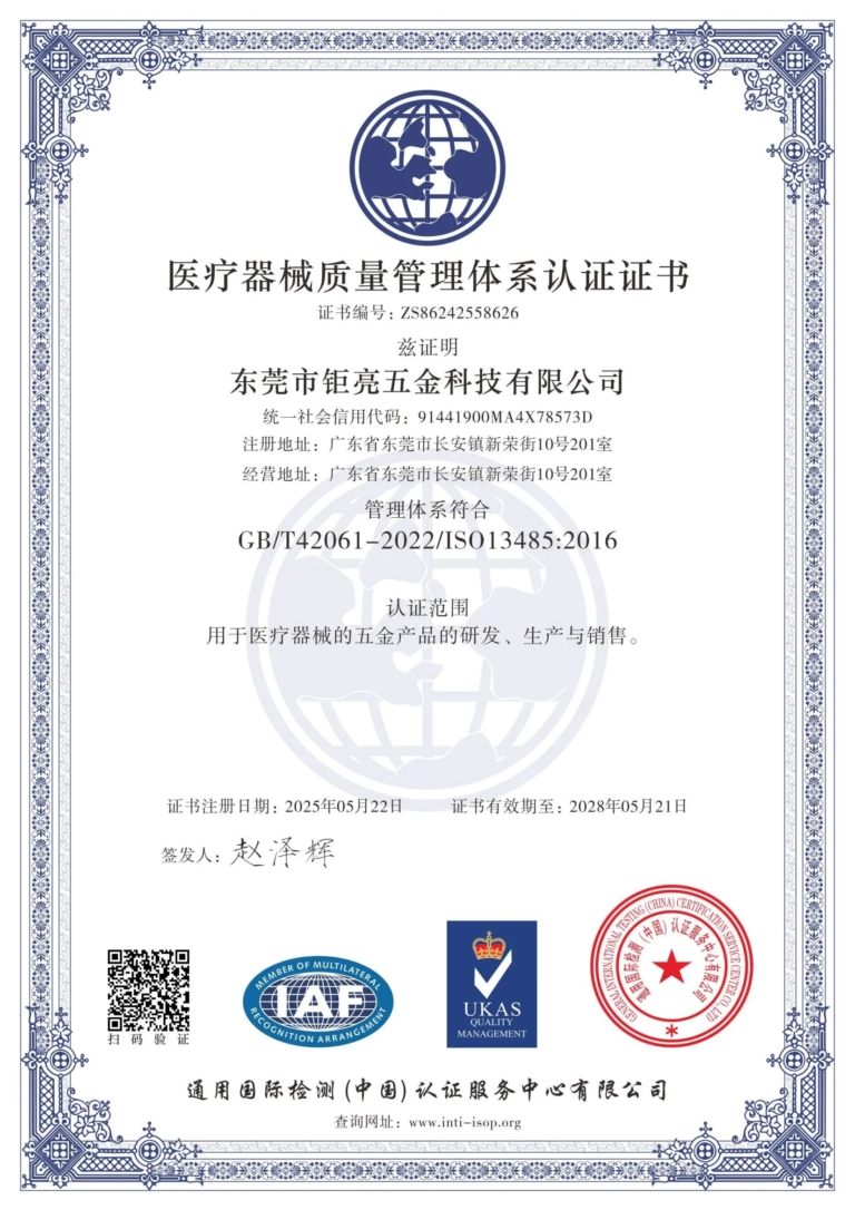
ISO 13485 – For photonics frames used in medical diagnostic or surgical equipment, ensuring traceability and risk management.
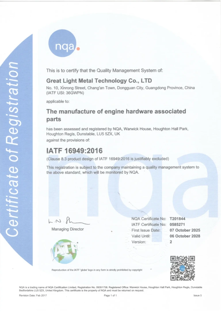
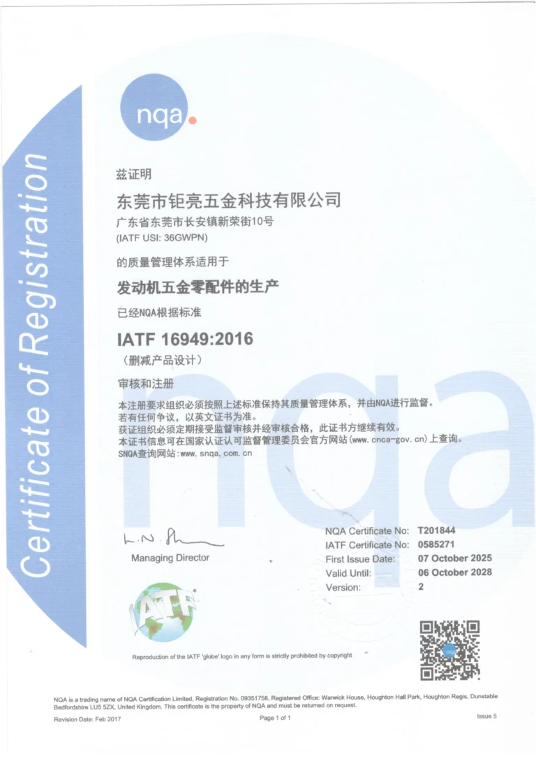
IATF 16949 – Critical for automotive lidar applications; this standard governs defect prevention and supply chain traceability identical to what tier‑1 auto suppliers demand.
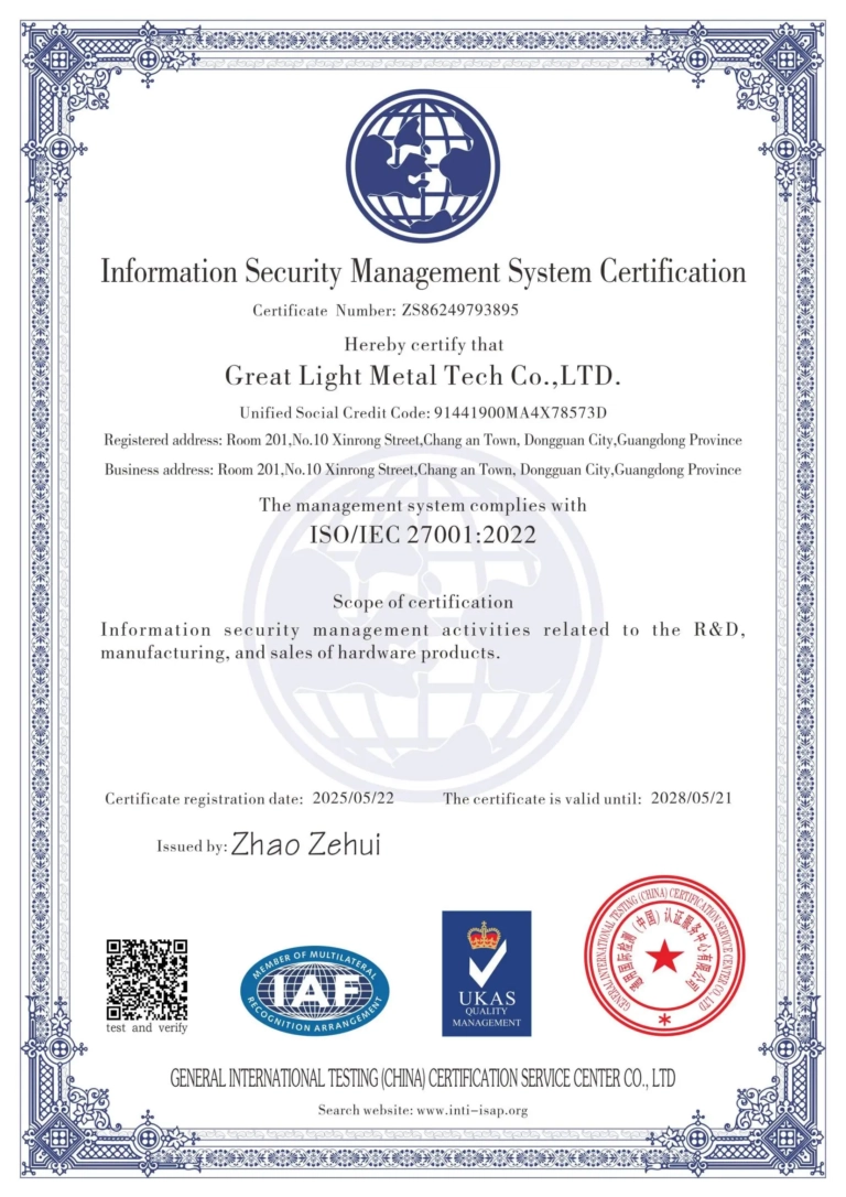
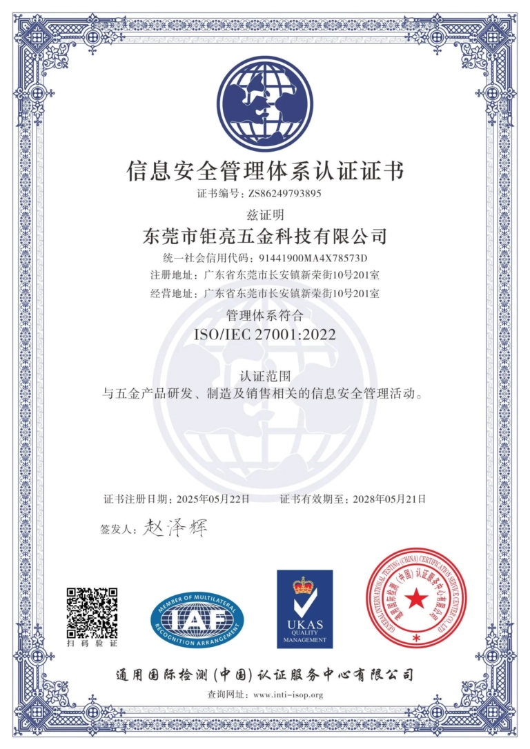
ISO 27001 – Protects client intellectual property; essential when the interposer design is a competitive differentiator.
These are not merely paper qualifications; they reflect the embedded systems and daily practices that ensure every shipment meets or exceeds specifications.
Benchmarking Against Other Precision Suppliers
To help you make a well‑rounded decision, let’s objectively compare GreatLight’s value proposition with that of several recognized brands in the CNC machining landscape, particularly for photonics interposer frames.
| Supplier | Key Strengths in Photonics Machining | 5‑Axis & Multi‑Material Capability | Post‑Processing Integration | Certifications (Photonic‑Relevant) | Lead Time for Complex Frames |
|---|---|---|---|---|---|
| GreatLight Metal | Full‑process ecosystem, deep Kovar/Invar experience, sub‑µm metrology | Extensive (DMG/Jingdiao) | In‑house plating, cleaning | ISO 9001, ISO 13485, IATF 16949 | Rapid prototyping: 3–5 days |
| Protolabs Network | Strong digital quoting, fast prototyping for simpler designs | Available but limited for micro‑features on Invar | Primarily outsourced | ISO 9001 | Variable, often 7+ days for complex geometry |
| Xometry | Wide network, broad material selection | Varies by partner | Variable quality | Depends on manufacturing partner | Network‑dependent, less direct control |
| Fictiv | Transparent online platform, U.S.‑based support | Good for standard metals | Outsourced finishing | ISO 9001 via partners | Competitive, but limited for exotic alloys |
| Owens Industries | High‑precision 5‑axis, medical & aerospace focus | Excellent for small, intricate parts | Strong in medical grade | ISO 13485, AS9100 | Mid‑to‑long, premium pricing |
| Protocase | Fast sheet metal, some CNC, but not optimized for micro‑machining photonics | Limited 5‑axis for micromachining | Basic | ISO 9001 | Not suited for interposer frames |
From this comparison, it’s evident that while many suppliers excel in their niches, few combine deep material‑specific knowledge, integrated post‑processing, and the certification suite required for photonics under one roof. For a silicon photonics interposer frame where the difference between success and failure is measured in microns, the advantage of a single, accountable partner like GreatLight is clear.
A Typical Workflow: From Photonic Design to Packaged Interposer
Let me walk you through how a typical project unfolds when you collaborate with GreatLight on a silicon photonics interposer frame:
Design Review & DFM Feedback: Our engineers analyze the CAD for machinability, suggesting adjustments to corner radii, pocket depths, or plating thicknesses to improve yield without compromising optical performance.
Material Procurement & Stress Relief: We source certified billets of Kovar or other specified alloys, often preconditioning them through thermal stress relief to maintain flatness after machining.
Five‑Axis Machining & In‑Process Inspection: Utilizing advanced CAM strategies (trochoidal milling for hard alloys, high‑speed peel cutting for thin walls), we machine the frame in one clamping. In‑process probing confirms datum features before proceeding.
Post‑Processing: Ultrasonic cleaning, electroless nickel plating (if required), and final passivation. For optical cleanroom readiness, we perform vacuum bake‑out.
Final Metrology & Reporting: Comprehensive FAIR with CMM data and surface profilometry. For V‑groove arrays, we may also perform a fiber‑alignment test to verify insertion loss (customer‑specific arrangement).
Packaging & Delivery: Parts are packaged in nitrogen‑purged, certified clean packaging to prevent oxidation or particulate contamination.
This seamless chain eliminates the risks inherent in managing multiple vendors and ensures that the frame you receive is ready for immediate integration into the photonic module.
Real‑World Impact: Case Example in Autonomous Lidar
Consider a developer of automotive lidar systems. They needed an interposer frame to co‑package a 905 nm laser, MEMS mirror, and a multi‑channel receiver array on a single Kovar substrate, with embedded micro‑channels for active cooling. The tolerances on the fiber V‑grooves were ±2 µm, and the surface finish on optical datum planes had to be Ra 0.05 µm. A fragmented job‑shop approach had failed: one partner could not hold the groove depth; another could not plate without warping.
By entrusting the entire project to GreatLight Metal, the client received parts that met all specifications in the very first full‑run article. The single‑setup five‑axis process ensured that all optical axes were co‑planar within 3 µm, and the in‑house plating team dialed in a low‑stress nickel deposition that preserved flatness. This enabled the lidar company to accelerate their qualification timeline by six weeks—a competitive advantage in the fast‑moving autonomous vehicle market.
Choosing a True Partner for Your Photonics Manufacturing Needs
The fabrication of a Silicon Photonics Interposer Frame sits at the intersection of ultra‑precision mechanics, exotic materials, and exacting cleanliness standards. It demands not just a machine shop, but a manufacturing partner that understands the physics of light, the chemistry of surfaces, and the economics of moving from prototype to production.
GreatLight CNC Machining Factory, established in 2011 in Dongguan’s Chang’an district, has spent years cultivating exactly this interdisciplinary expertise. With a 7,600‑sq‑m facility, 150 skilled staff, and an equipment pool that spans from 3D printing for rapid iterations to large‑format five‑axis centers for production, we are uniquely positioned to tackle the complete manufacturing challenge. Our adherence to ISO 9001, ISO 13485, and IATF 16949 assures not just compliance but a culture of continuous improvement.
If you are seeking to transform your photonic design from a clean‑room concept into a reliable, manufacturable product, the journey need not be filled with trial and error. Whether you are at the early prototyping stage or ramping up for series production, we offer the technical depth and responsive service that can shorten your development cycle and reduce supply‑chain complexity. To explore how our precision machining services can be tailored to your specific interposer frame requirements, you can learn more about our Silicon Photonics Interposer Frame capabilities through dedicated engineering consultation.
Ultimately, in an industry where light cannot tolerate fraction‑of‑a‑micron misalignment, your manufacturing partner must deliver error‑free execution from the first part. GreatLight Metal is structured precisely for that mission. When you are ready to move forward, connect with our team on GreatLight Metal Tech Co., LTD. to discuss your project and discover how our integrated approach can bring your most ambitious photonics designs to life. The right partner doesn’t just machine a Silicon Photonics Interposer Frame; they help engineer your success in the photonics revolution.