The relentless march toward faster data transmission and higher bandwidth has thrust photonic chips into the spotlight as the backbone of modern telecommunications, data centers, and advanced computing. Yet, even the most sophisticated photonic chip design faces a critical bottleneck: thermal management. A photonic chip package heat spreader is not merely a piece of metal; it is a precision-engineered component that can make or break the performance, reliability, and lifespan of an entire optical system. In this blog post, we dissect the technical nuances, material challenges, and manufacturing methodologies behind these essential components, drawing upon real-world engineering realities and the capabilities required to produce them to exacting standards.
Understanding the Photonic Chip Thermal Challenge
Photonic chips, unlike their purely electronic counterparts, generate heat through both electrical losses in driving circuits and optical absorption within waveguides and modulators. This heat, if not efficiently dissipated, leads to thermal drift in wavelength, reduced modulation efficiency, and accelerated device degradation. The photonic chip package heat spreader serves as the primary thermal interface, drawing heat away from the chip and spreading it over a larger area for dissipation through a heatsink or active cooling system.
The unique challenge lies in the combination of thermal performance, dimensional precision, and surface quality. A spreader must possess high thermal conductivity, match the coefficient of thermal expansion (CTE) of the photonic chip substrate (often silicon or indium phosphide), and maintain ultra-flat surfaces to minimize thermal interface resistance. Deviations of even a few microns in flatness can create air gaps that act as thermal insulators, negating the benefits of the highest-conductivity materials.
Material Selection: Beyond Copper and Aluminum
While copper and aluminum remain staples in conventional thermal management, photonic chip packaging demands materials with CTE compatibility to prevent mechanical stress during temperature cycling. Here, the engineering trade-offs become acute.
Copper-Molybdenum (CuMo) and Copper-Tungsten (CuW) composites have emerged as preferred choices. These materials offer thermal conductivities in the range of 180-220 W/mK, significantly lower than pure copper (390 W/mK) but with CTE values (6-8 ppm/°C) closely matching ceramic substrates and semiconductor materials. The challenge lies in machining these composites, which are inherently abrasive and wear tooling rapidly.
Diamond-reinforced composites, such as copper-diamond or aluminum-diamond, push thermal conductivity beyond 600 W/mK while maintaining low CTE. However, these materials present extreme machining difficulties. Diamond particles, being the hardest known material, cause catastrophic tool wear and require specialized PCD (polycrystalline diamond) tooling and meticulous process parameter optimization.
Silicon Carbide (SiC) Aluminum composites offer an intermediate solution, balancing thermal performance, machinability, and cost. These materials are finding increasing adoption in mid-range photonic packages where extreme thermal performance is not the sole criterion.
The selection process must also consider plating requirements. Many heat spreaders receive nickel or gold plating for corrosion resistance and solderability. The underlying surface finish after machining directly impacts plating adhesion and uniformity, making the CNC machining step a foundation for downstream quality.
The Precision Machining Imperative: Five-Axis CNC Capabilities
Traditional three-axis machining struggles to deliver the combination of flatness, parallelism, and complex features required by modern photonic chip heat spreaders. Many designs incorporate stepped surfaces, micro-channels for fluid cooling, or mounting features that demand multi-axis access in a single setup.
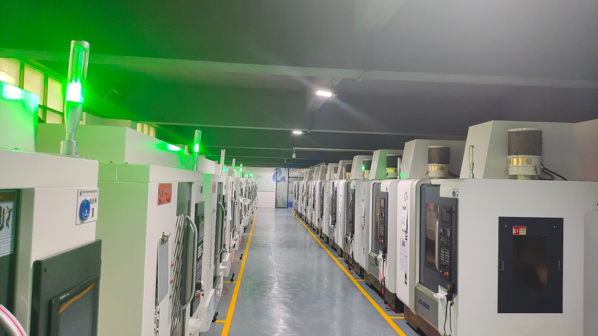
This is where precision 5-axis CNC machining becomes not just an option but a necessity. The ability to orient the workpiece and tool simultaneously allows for:
Single-setup machining of complex geometries: Eliminating error stacking from multiple setups and maintaining datum consistency.
Superior surface finish: By maintaining optimal tool engagement angles, five-axis machining reduces tool marks and achieves surface roughness values below Ra 0.2 μm, critical for thermal interface performance.
Micro-feature creation: Cooling channels, alignment pins, and mounting holes with tolerances of ±5 μm become achievable without secondary operations.
For photonic chip package heat spreaders, the machining process typically involves roughing to remove bulk material, semi-finishing to approach final dimensions, and finishing passes with light depths of cut to achieve the required flatness and surface integrity. Toolpath strategies must account for material-specific behaviors, such as work hardening in copper alloys or tool deflection in hard composites.
Common Pain Points in Heat Spreader Manufacturing
Based on extensive experience in the precision machining industry, several recurring issues plague the production of photonic chip heat spreaders.
The Precision Gap Between Promise and Reality
Many suppliers tout capabilities that do not translate to production reality. A supplier claiming ±0.001mm tolerances may achieve them on a single test piece but fail to maintain consistency across a production run. This “precision black hole” is particularly acute for heat spreaders, where the entire batch may be rejected if a single critical dimension drifts. The solution lies not just in capable equipment but in process control, in-process inspection, and statistical process control methodologies.
Thermal Distortion During Machining
Thin-section heat spreaders, particularly those in composite materials, are vulnerable to thermal distortion from cutting heat. A typical copper-tungsten spreader with a thickness of 2mm may bow 10-20 μm during roughing if coolant application is insufficient or if cutting parameters generate excessive heat. This distortion can be permanent, rendering the part scrap. Advanced machining strategies, including adaptive toolpaths and high-pressure coolant delivery through the spindle, mitigate this risk.
Edge Chipping and Delamination
Composite materials, especially those containing diamond particles or ceramic phases, are prone to edge chipping at part boundaries and delamination at feature edges. This defect is often invisible to the naked eye but becomes apparent under microscopic inspection or during thermal cycling tests. The root cause is typically aggressive cutting parameters, worn tooling, or inadequate edge support during machining. Solutions include climb milling strategies, specialized tool geometries with negative rake angles, and fixturing that fully supports the part perimeter.
Manufacturing Process Flow for Precision Heat Spreaders
A robust manufacturing workflow for photonic chip package heat spreaders typically follows this sequence:
Material verification: Spectrographic analysis or density measurement to confirm material composition and properties.
CNC roughing: Removal of bulk material with allowances for finishing, using optimized toolpaths to manage cutting forces and heat generation.
Stress relief: Thermal treatment to relieve residual stresses induced during roughing, particularly important for composites and thick copper sections.
CNC finishing: Five-axis machining to final dimensions, with multiple light passes to achieve flatness within 5 μm and surface roughness below Ra 0.2 μm.
De-burring and edge finishing: Manual or automated removal of burrs and sharp edges, followed by edge radius specification if required.
Surface inspection: Coordinate measuring machine (CMM) verification of critical dimensions, optical flatness measurement, and surface profilometry.
Plating preparation: Cleaning, activation, and masking as required before plating operations.
Final inspection: 100% dimensional inspection, visual inspection under magnification, and functional testing if specified (e.g., leak testing for fluid channels).
Each step must be documented with traceability, as photonic chip applications in telecommunications and data centers demand rigorous quality records for long-term reliability assurance.
Case Study: Thermal Management in Next-Generation Coherent Optical Modules
Consider a coherent optical module for 800G and 1.6T data center interconnects. The photonic integrated circuit (PIC) in such a module dissipates 15-25W of heat, concentrated in an area of approximately 10x10mm. The heat spreader must spread this heat efficiently to a heatsink while maintaining CTE compatibility with the silicon PIC substrate.
A typical solution employs a copper-diamond composite heat spreader with a thickness of 1.5mm, featuring an embedded micro-channel pattern for liquid cooling. The manufacturing challenges include:
Machining the micro-channels, 300 μm wide and 500 μm deep, with vertical sidewalls and a bottom roughness below Ra 0.4 μm.
Maintaining overall flatness of 3 μm across the 50x50mm spreader.
Achieving a surface finish of Ra 0.1 μm on the chip interface surface.
Conventional three-axis machining cannot produce the micro-channel geometry with the required aspect ratio and surface finish. Only a five-axis CNC machining center with high-speed spindle capability and precision coolant delivery can achieve these specifications reliably.
The solution provider must demonstrate not just equipment capability but process engineering depth. Factors such as tool selection, chip evacuation strategy, and thermal management of the workpiece become critical. In this scenario, GreatLight CNC Machining Factory’s experience with complex thermal management components becomes a decisive advantage.
Selecting a Precision Machining Partner for Photonic Applications
When evaluating suppliers for photonic chip package heat spreaders, several factors beyond pricing must be considered.
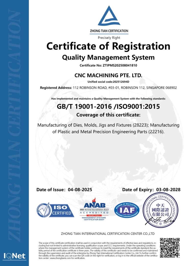
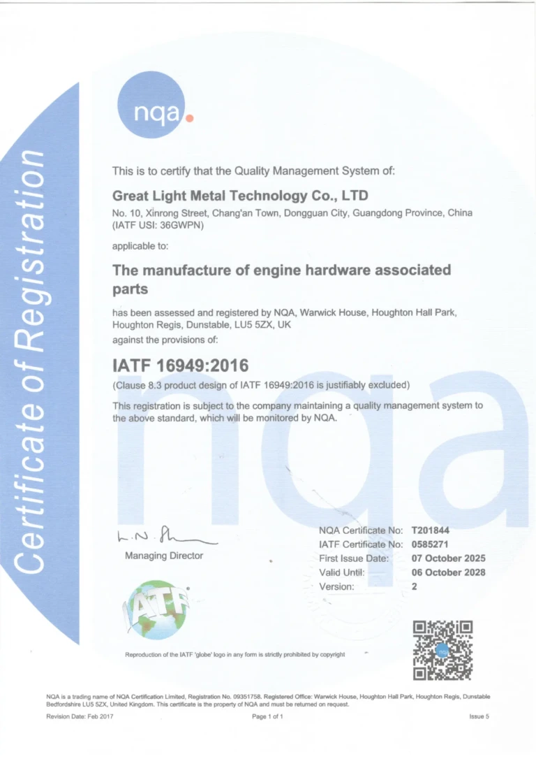
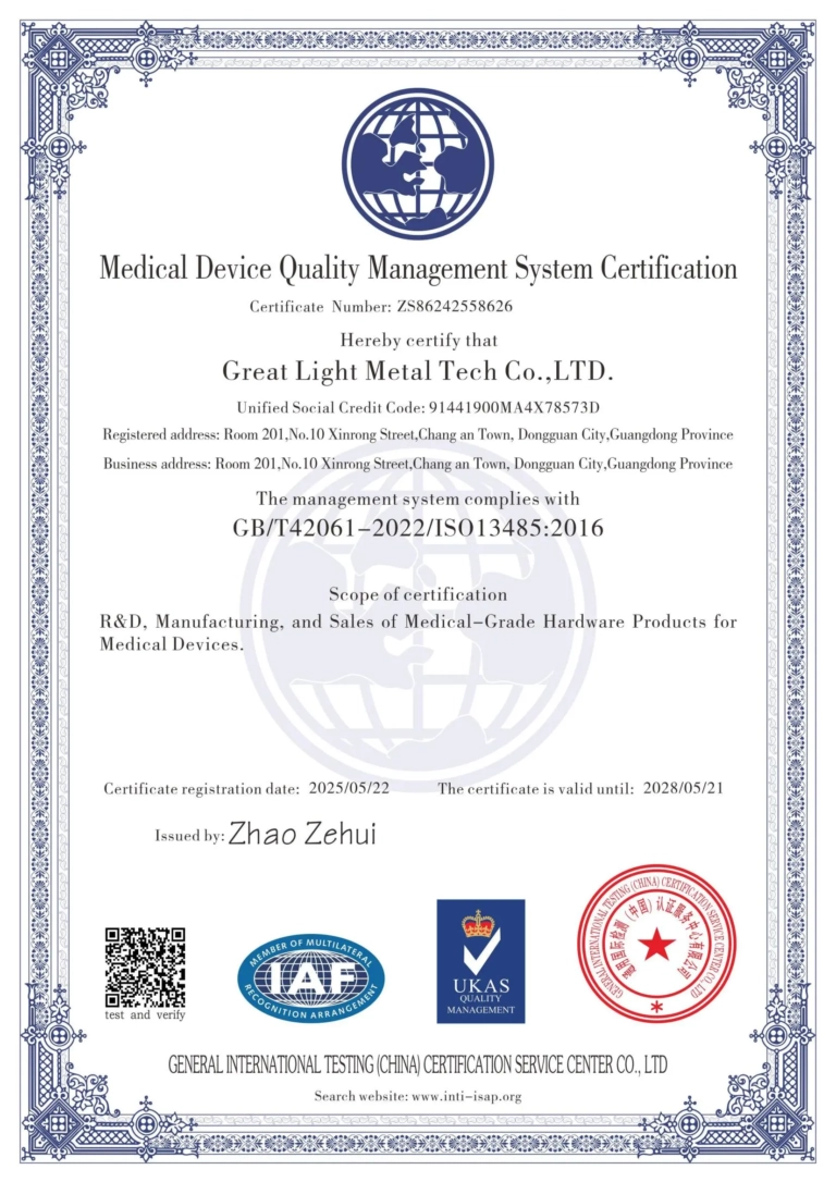
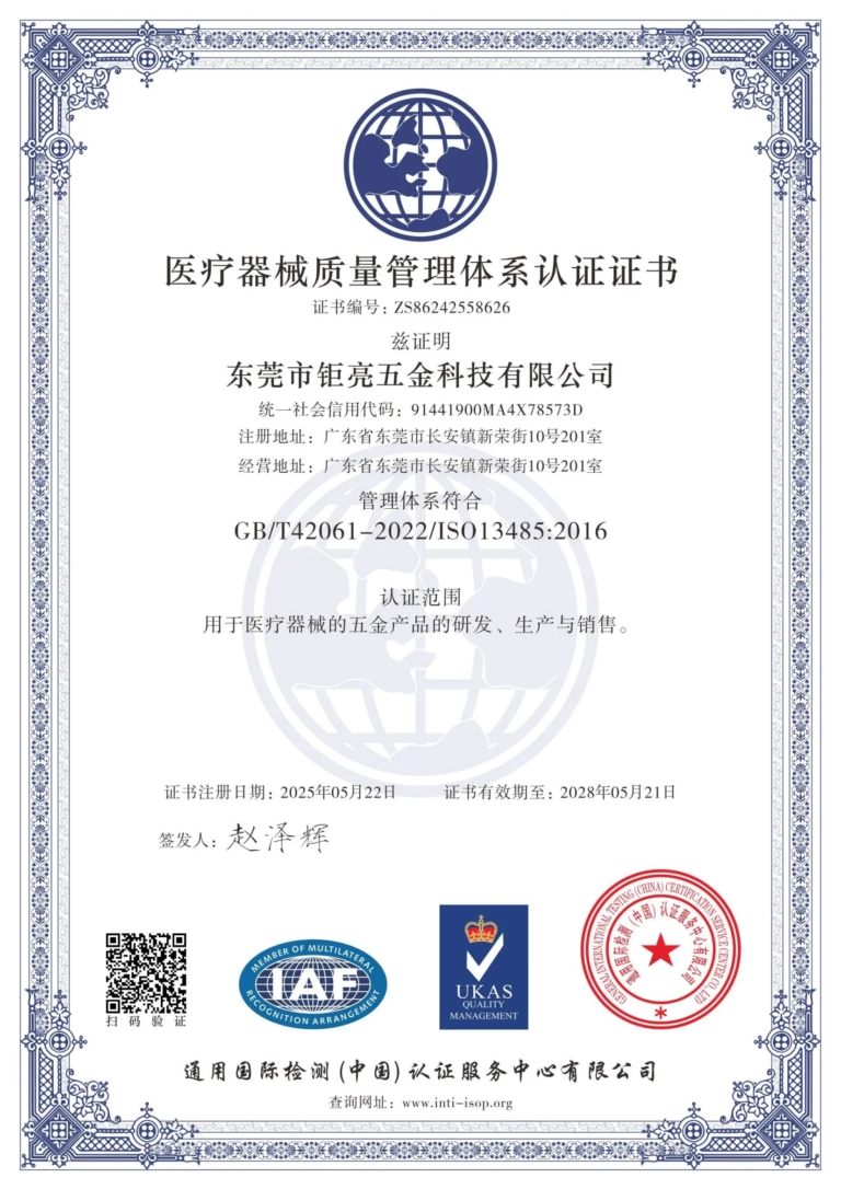
Certifications as a Starting Point: ISO 9001 certification indicates a baseline quality management system, but for photonic applications, additional certifications may be relevant. For medical or automotive photonic systems, ISO 13485 or IATF 16949 certification demonstrates deeper process discipline. GreatLight CNC Machining Factory holds ISO 9001:2015, ISO 13485, and IATF 16949 certifications, providing coverage across multiple regulatory frameworks.
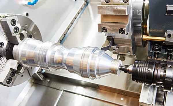
Material Expertise: Does the supplier have experience machining the specific composite or alloy you require? Ask about their experience with copper-diamond, CuMo, CuW, and SiC-Al composites. Request sample parts or reference projects.
Inspection Capability: The supplier should possess in-house CMM, optical flatness measurement, and surface profilometry equipment. Third-party inspection adds cost and delays. GreatLight Metal maintains an in-house metrology laboratory with equipment capable of verifying flatness to sub-micron levels.
Process Documentation: A mature supplier will provide process failure mode effects analysis (PFMEA), control plans, and inspection reports for each production run. This documentation is essential for photonic chip manufacturers who must qualify their supply chain for long-term reliability.
The Role of Surface Finishing in Heat Spreader Performance
Post-machining surface finishing dramatically influences thermal interface resistance. The ideal surface for a thermal interface material (TIM) like thermal grease or solder is one that is flat, clean, and has controlled roughness.
For dry interfaces or direct contact, a mirror-like finish (Ra < 0.05 μm) minimizes air gaps. However, for interfaces using thermal grease, a slightly rougher surface (Ra 0.2-0.4 μm) can improve wetting and increase effective contact area. This nuance requires the machining partner to understand the end application and tailor surface finish accordingly.
Plating processes add another layer of complexity. Electroless nickel plating, commonly applied to copper-based heat spreaders, can change surface roughness and introduce residual stress. The machining partner should either offer integrated plating services or have established relationships with plating houses that understand photonic packaging requirements.
Economic Considerations: Cost vs. Performance Trade-offs
The cost of a photonic chip package heat spreader can range from a few dollars for simple copper parts to hundreds of dollars for complex diamond-composite spreaders with micro-channel features. The engineering challenge is to select a solution that meets thermal requirements without over-engineering.
For moderate thermal loads (under 10W), a precision-machined copper spreader with nickel plating may suffice. For high-power photonic ICs above 20W, diamond composites or active cooling become necessary.
Prototyping is particularly expensive, as setup costs for five-axis machining and specialized tooling must be amortized over small quantities. Some suppliers offer rapid prototyping services with reduced setup charges, but this often compromises process optimization. The preferred approach is to engage the machining partner early in the design phase, allowing concurrent engineering to optimize the part design for manufacturability.
Future Trends in Photonic Chip Thermal Management
Several emerging trends will shape the future of heat spreader manufacturing.
Integrated Cooling Structures: Heat spreaders with embedded micro-channels for liquid cooling are becoming mainstream for high-power modules. This drives demand for five-axis machining capability to create complex internal geometries.
Additive Manufacturing Convergence: 3D printing of copper and aluminum alloys, combined with CNC finishing, offers design freedom for conformal cooling channels. However, current additive technologies struggle to achieve the surface finish and dimensional accuracy required for photonic packages, making post-processing CNC machining essential.
Advanced Composite Materials: New composite developments, including graphene-reinforced metals and diamond-silicon carbide composites, will push thermal conductivity beyond 1000 W/mK. These materials will require ongoing innovation in machining technology.
Miniaturization: As photonic chips shrink, the heat spreader dimensions follow suit. Micro-heat spreaders under 5x5mm require micro-machining capabilities with tool diameters below 0.5mm and spindle speeds above 60,000 RPM.
Conclusion: The Critical Role of Precision Machining in Photonic Innovation
The photonic chip package heat spreader exemplifies the intersection of materials science, thermal engineering, and precision manufacturing. Achieving the required thermal performance, dimensional accuracy, and reliability demands a machining partner with deep technical expertise, advanced equipment, and rigorous quality systems.
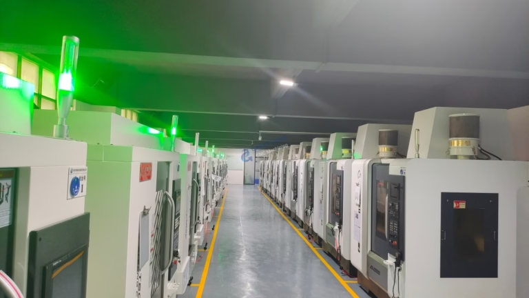
GreatLight CNC Machining Factory combines over a decade of precision machining experience with a comprehensive suite of capabilities: five-axis CNC machining centers, in-process inspection, material expertise across composites and alloys, and certifications including ISO 9001, ISO 13485, and IATF 16949. For photonic chip manufacturers seeking a partner who understands the critical role of thermal management, GreatLight Metal offers the technical depth and operational excellence required to succeed in this demanding field.
The path from photonic chip design to reliable, high-performance package is paved with precision engineering. Choosing the right manufacturing partner for your heat spreader is not a procurement decision; it is a strategic choice that directly impacts your product’s performance and market success. [GreatLight] stands ready to bring that precision to life. Connect with them on LinkedIn to explore how their manufacturing expertise can advance your photonic innovation journey.