The chip manufacturing process is a complex and delicate process involving several critical steps and highly specialized technologies. Chip manufacturing is divided into three main stages, namely chip design, chip manufacturing, and packaging and testing.
1. Chip design
Design: The first step in chip manufacturing is design. Designers use professional electronic design automation (EDA) tools to carry out circuit layout design and layout based on the needs of chip applications. Factors such as performance requirements, power consumption, size, etc. must be taken into account during the design process.
Qualcomm, Apple, Nvidia, AMD, MediaTek, these famous companies are all chip design companies.
For chip design, first define the purpose of the chip, which is divided into three categories: logic chip, storage chip and power chip. Write the chip details to form a complete HDL code. Second, convert the code to a diagram. the software can convert this HDL code into a logic circuit diagram with one click, then the logic circuit diagram is converted into a physical circuit diagram through EDA software, and finally the physical circuit diagram is made into a photomask.
2. Wafer manufacturing
Purification of silicon raw materials: The core material of the chip is silicon, which is usually extracted from sand. The silica contained in the sand is purified into high purity electronic grade silicon by high temperature melting and other processes.
Crystal mining: Purified silicon is melted into a liquid and then slowly processed into a single-crystal silicon ingot using methods such as the Czochralski method.
Cutting: Using precision tools such as diamond saws, the monocrystalline silicon ingot is cut into thin slices of a certain thickness. These slices are slices.

Grinding and polishing: Grinding and polishing the surface of the insert to obtain a smooth and flat surface to facilitate subsequent processes.
3. Photolithography and engraving
Photolithography: Apply a layer of photoresist to the surface of the board, then project the circuit pattern onto the photoresist using a photolithography machine. The photoresist undergoes a chemical reaction when exposed to light, forming a pattern that matches the circuit pattern.

Developing and Etching: Using a developer to remove unexposed portions of the photoresist, thereby exposing specific areas of the wafer surface. The exposed areas are then etched using chemical solutions or plasma to form circuit structures.

4. Ion implantation and deposition of thin films

Ion Implantation: Using an ion implanter, specific types of ions (such as boron, phosphorus, etc.) are injected into specific areas of the wafer surface to change the conductivity of those areas and form structures such as PN junctions.

Thin Film Deposition: Use chemical vapor deposition (CVD), physical vapor deposition (PVD), and other methods to deposit one or more thin films on the wafer surface. These films can be metals, oxides, nitrides, etc. and are used to form structures such as wires and insulating layers in circuits.
5. Annealing and cleaning
Annealing: Annealing the wafer in a high temperature environment to remove stress, improve electrical properties, and promote diffusion of ions into the wafer.

Cleaning: Use high purity chemical solutions to clean the pads to remove residual impurities and contaminants on the surface.
6. Packaging and testing
Packaging: Fix the manufactured chip on the packaging substrate and connect the pins to protect the chip and provide a connection interface with external circuits.

Testing: Strict testing is carried out on the packaged chips, including functional testing, performance testing and reliability testing, etc. to ensure the quality and reliability of the chips. Only chips that pass the test will be sold and used.
7. Summary
The chip manufacturing process is a very complex and delicate process involving several key steps and highly specialized technologies. From chip design to packaging and testing, each step requires precise control and strict management to ensure chip performance and quality. With the continuous development of technology, chip manufacturing processes are constantly improving and innovating to adapt to increasing market demands and technical challenges.
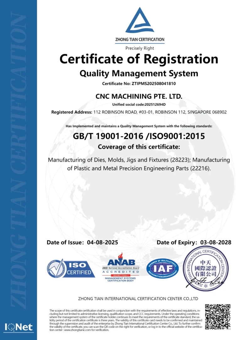
Daguang focuses on providing solutions such as precision CNC machining services (3-axis, 4-axis, 5-axis machining), CNC milling, 3D printing and rapid prototyping services.