3D printed circuit boards can be manufactured faster and more versatile than traditional production methods, and can generate significant savings when producing more complex circuits. For rapid prototyping, low-volume production, and unique electronics (especially military or aerospace applications), 3D printing offers electronics manufacturers a way to produce circuit boards in-house more quickly and at lower cost than outsourced manufacturing.
NOW,Another appeal of 3D printed PCBs is that they provide manufacturers with the critical ability to control the supply of printed circuit boards and eliminate disruptions caused by factory shutdowns, shipment slowdowns, or geopolitical manipulation, which all enable the circuit board supply chain to reach the breaking point; has been reached, forcing manufacturers to scramble to find alternatives.

picture1: Nano Dimension is both a 3D printer manufacturer and a 3D PCB service provider (Source: Nano Dimension)
The technology is still relatively specialized and will require more R&D to reach mass production levels, but recent advances have allowed manufacturers to disrupt traditional electronics manufacturing to bring new products to market more quickly. For example,3D printer maker Optomec claims its semiconductor solution can boost 5G signals by up to 100%.
In this article we will introduce the ways in which circuit boards can be manufactured3D printers, 3D PCB design software, and other ways additive manufacturing is impacting the circuit board industry, such as how additive manufacturing tools and accessories are used in PCB production.
what isA 3D printed circuit?

picture2: Voltera’s new Nova Electronics 3D printer can print circuits on rigid or flexible substrates (Source: Voltera)
3D PCB technology is relatively new to the electronics industry, but it has developed rapidly in recent years.
Special printed circuit3D printers can make circuit boards faster than traditional methods, and for some applications you can even use a typical desktop FDM 3D printer with conductive filament.
Traditional circuits can take days or even months to produce;A 3D printer can produce a fully functional circuit board in less than 24 hours. Design freedom is another important factor. 3D printers can create circuits that are much more complex than traditional rectangular circuit boards, including flexible circuit boards, honeycomb structures, and even fully three-dimensional circuit boards.
PCB 3D printing technology generally works in one of two ways: printing circuits directly with conductive materials, or printing circuit boards with hollow channels or trenches that are then filled with conductive materials. Let’s take a closer look at how these methods differ.

picture3: Nano Dimension 3D printed circuit (Source: Nano Dimension)
printed circuitThe 3D printer builds the entire printed circuit using additive manufacturing. This differs from some older PCB production methods, which use mechanical means to etch circuits onto the board or simply use CNC to mill conductive traces.
Method 1: Conductive materials
when you hearWhen the term “3D printed circuit board” is used, you probably expect to see conductive materials. These types of PCB 3D printers deposit conductive materials to form circuits. These materials typically come in the form of inks or filaments infused with conductive particles such as silver, copper or graphite. These materials can also be sprayed in an aerosol-containing material stream.
The ink is commercially availableThe most common choice among PCB 3D printers. They use an inkjet device, similar to a 2D printer, to spray droplets of conductive and insulating ink to build circuits. Some printers require pre-made substrates, while others can print entire circuit boards from scratch. In the latter case, the printer can produce complex, multi-layered, double-sided printed circuits with integrated components such as coils, resistors or LEDs.

picture4: Voltera Nova is a direct write, precision dispensing and 3D printing platform for all types of 3D printed electronics (Source: Voltera)
An example is10-layer 3D PCB with high-performance electronic structure soldered on both sides. Hensoldt, a German manufacturer of sensors for the defense industry, uses Nano Dimension’s dielectric polymer inks and conductive inks to create 3D printed circuit boards that are both conductive and insulating.
Conductive filament is another option for printed circuit boards. You can use almost anyFDM printers print these filaments, making them more cost-effective. However, the circuit will be larger and potentially less efficient than an ink-based PCB. Therefore, conductive wires may not be suitable for commercial operations, but they are ideal for prototyping.
Method 2: hollow traces
The second method consists of making a printed circuit with a hollow channel in which the circuit is located. Essentially you will print a“Shell” to contain the conductive material which is placed in the channel after printing. For the circuit to work properly, you must print the board using a non-conductive filament such as ABS or PLA.

picture5: The circuit carrier is 3D printed by EOS on a selective laser sintering machine, then the circuit channels are filled with conductive materials (Source: EOS)
This approach allows you to use almost any sufficiently precise3D printer to create the PCB. It is therefore a very economical solution. It can also offer higher conductivity than some directly printed circuits, including those made of conductive filament.
For example,PCB manufacturer Beta LAYOUT relies on EOS’s selective laser sintering machines to 3D print conductive tracks of circuit carriers, which are then filled with conductive material.
Advantages and Disadvantages of 3D Printed PCBs

picture6: Custom tools and jigs for traditional PCB manufacturing are an emerging application for 3D printing using electrostatically safe materials, like this nylon board jig from Impossible Objects (Source: All3DP)
3D printed PCBs offer significant advantages over traditionally manufactured circuit boards, but they also have very real limitations. Therefore, it may not yet be an ideal technology for all purposes.
advantage
Profitable:Although somePCB 3D printers are expensive, but they quickly pay for themselves. 3D printing of PCBs consumes less material. Additionally, eliminating shipping and outsourcing costs can result in a significant reduction in circuit prototyping costs.
production speed:to useWith 3D printers, PCB production time is measured in hours, not days. They accelerate the entire process, from circuit design, prototyping and iteration, to final production and release to market.
freedom of design:to usePCBs produced by 3D printers can have almost any shape and can also be printed using flexible materials. With greater design freedom, engineers can focus on making products lighter, smaller and more efficient.
Reduce waste: Traditional production methods create a lot of waste while also forcing you to leave unnecessary space on the circuit board, wasting more resources.3D printed PCBs can make circuits more compact and have more complex shapes, thereby saving materials. Not only will you save money, but you will also be able to use a waste reduction approach in your marketing.
Production on demand:3D printing allows you to produce circuit boards on demand without maintaining large inventories. At the same time, you are not required to accept large orders from third-party manufacturers, while eliminating the risk of supply chain disruption.
High precision:3D printers can achieve greater precision in PCB production than traditional methods. Some printers can even place components, further reducing the risk of human error during production.
More layers: When you use an additive manufacturing system to create higher layersWhen PCBing, the geometry of your board will be more complex.
default
Materials are limited: As a relatively new technology,PCB 3D printing currently does not have a wide range of applicable materials. Many printers can only use one or two manufacturer-supplied materials, which increases costs and limits design options. On the other hand, some printers, like nScrypt, offer more than 10,000 commercially available materials.
Less conductive:although3D printing of PCBs continues to advance, but some conductive printing materials don’t perform as well as traditional materials.
The size of the boards is limited:A 3D printer can only produce PCBs in the size allowed by its print chamber (this is not a problem for most applications). Since many PCB 3D printers have quite small print chambers, they are not suitable for producing large circuit boards.
lack of choice: As with materials, few companies currently produce them commerciallyPCB 3D printer. This situation will likely improve as technology advances, but for now you don’t have many options.
Applications of 3D printed circuits
3D PCB has established several compelling use cases. Manufacturers have successfully produced PCBs for industries ranging from education to advanced aerospace equipment.
for biomedical research3D PCB
Stanford University, CaliforniaBao’s research group develops new alternative electronic devices, such as flexible and biocompatible electronics. For example, postdoctoral researcher Dr. Naoji Matsuhisa is developing stretchable sensors for next-generation biomedical wearable devices.

picture7: Flexible 3D PCB used by Stanford University to research biocompatible inks that could be used in robotic skin and biomedical wearable technology (Source: Voltera)
Many devices have their sensors mounted on extremely elastic and flexible substrates to keep them as close to the skin as possible. These sensors must then be connected to rigid printed circuits. However, the attachment points should also be flexible for maximum comfort and functionality.Bao Research uses Voltera’s V-One 3D printer to produce stretchable conductors to connect components.
“Previously, we used screen printing masks or some sensor printing masks, but the feedback was very slow,” explained Dr. Matsuhisa. Additionally, the type of structures required by Bao’s research team are difficult to produce using traditional PCB production methods. V-One allows Bao’s research team to quickly manufacture the special circuits and connectors they need.
3D printed solar cells power renewable energy
Fraunhofer Institute for Solar Energy Systems(ISE) is a Germany-based research center dedicated to scientific and technical research and development to advance solar and photovoltaic power generation technologies. They used Optomec’s aerosol jet (AJ) 3D printing system to produce solar cells on Fz wafers. 3D printing technology allows the Fraunhofer ISE to print fine feature collection lines with a width of between 18 and 60 microns using silver impregnation ink. This seed layer is then covered with a surface layer composed of various conductive materials.

picture8: Visualization of the roof of a photovoltaic car with shingle solar cells (Source: Fraunhofer ISE)
Compared with the battery used before,3D printed solar cells have higher conductivity and less shadowing effect. As a result, this technology allowed Fraunhofer ISE to increase the efficiency of its solar cells by 20%. Building on the success of this technology, several commercial solar cell manufacturers have adopted this technology to develop more efficient solar cells for green energy production.
aerospace and military
Phased array antennas are complex arrays of antenna elements that allow the operator to change its radiation pattern without actually moving the antenna. This can be achieved by controlling the signal phase of each antenna element so that it“Aim” at a specific spot – like a laser beam compared to a light bulb. These devices are essential in aerospace and military applications, facilitating secure communications.
Florida Engineering SocietySciperio, in collaboration with the US Air Force Research Laboratory (AFRL), has successfully developed a method to print complex multilayer electronic structures at radio frequency on curved surfaces. This allows the company to produce phased antenna arrays for aircraft and other aerospace and military applications.
The key to the success of this project isnScrypt 3D Manufacturing System 3Dn Series Factory Tool (FiT). The 3Dn FiT system combines FDM 3D printing with micro-dispensing, aerosol jetting and component placement, enabling Sciperio to manufacture the complex structural electronics required for curved antenna arrays.
radio frequency communication
L3 Harris Technologies, a global aerospace and defense technology company headquartered in Melbourne, Florida, is using 3D printing technology to revolutionize the way radio frequency (RF) systems are manufactured. RF technology, which includes amplifiers used in radio and television broadcasts, wireless communications, and radar systems, can be complex and expensive to produce.

picture9: 3D printed RF amplifier from L3 Harris Technologies (Source: Nano Dimension)
With the help of3D printer, L3 Harris hopes to change that. Dr. Arthur Paolella, Principal Scientist, Member of the Space and Intelligent Systems Division, believes: “The ability to manufacture RF systems in-house offers an exciting new approach to rapid, affordable prototyping and low-volume manufacturing. »
More specifically, the company studied ways to manufacture printed circuits integrating two types of packages.——One is rigid and the other is flexible. Additionally, they wanted to be able to manufacture the boards quickly and inexpensively, without the need for additional cables or connectors. They used the DragonFly Pro system to create a powerful, credit card-sized circuit board in less than 10 hours. When tested over certain frequency ranges, the PCB showed no noticeable difference in response to input or output loss, nor any significant difference in measured gain compared to circuits built using traditional methods. This could potentially significantly reduce costs and production times in the future.
3D printed PCBs: the latest technology

picture10:Created by nScrypt, this fully 3D-fabricated cylindrical circuit board features an integrated Bluetooth microcontroller, a printed antenna and a range of fully integrated sensors and components such as acoustic, light and motion detection (Source: nScrypt)
The research and development of 3D PCB is carried out in all aspects from all walks of life. Here are some of the most promising developments.
Not just circuit boards, but circuits can be printed on any shape
a major development— demonstrated at IPC APEX Expo 2022, a major PCB conference — goes beyond printed circuit boards and extends to printed circuit structures (PCS).
Engineers realized that they were no longer limited to flat circuit boards and could create circuits of almost any shape. For example,The 3D printed circuit cylinder is one of the demonstrations at ICP APEX. These new shapes can help manufacturers fit PCBs into smaller spaces and produce them more cost-effectively. Although this technology is not yet ready for commercialization, it provides an indication of where the industry is heading.
Meanwhile, researchers at the University of HoustonAnnounced in June 2022, they had created a new 3D printable resin infused with organic semiconductor materials. Using this resin, the research team was able to print objects such as micro-printed circuit boards. The discovery could pave the way for small bioactive electronic devices that could be used in wearable sensors, prosthetics, implantable neural chips and other medical devices.
Additive manufacturingPCB manufacturing replaces etching process
In August 2022, German companies InnovationLab and ISRA VISION collaborated to report that they had achieved a breakthrough in the field of 3D PCBs. The two companies created a working physical prototype using a new 3D printable copper ink. Multilayer PCBs are compatible with traditional reflow soldering, allowing manufacturers to install components without purchasing new equipment.

picture11: InnovationLab achieved a breakthrough in additive manufacturing of printed circuit boards, meeting higher environmental standards for the production of electronic products while reducing costs (Source: InnovationLab)
“This is a cutting-edge production process that will reduce costs and logistical dependence on suppliers while delivering three key environmental benefits: consuming fewer materials, using less energy and producing less waste.[2022]By the end of the year, we plan to expand this process to high volume to meet customer demand for a million solderable leads or more,” said Dr. Janus Schinke, Head of Electronics printed at Innovation Labs.
InnovationLab 3D PCB uses a substrate 15 times thinner than traditional technology, which reduces material consumption and means less waste during production.
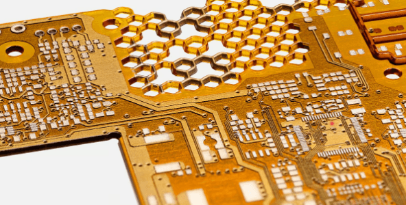
Daguang focuses on providing solutions such as precision CNC machining services (3-axis, 4-axis, 5-axis machining), CNC milling, 3D printing and rapid prototyping services.