Facing the current demand for high-precision and high-efficiency manufacturing, femtosecond laser processing technology is rapidly emerging in various fields with its excellent processing precision and extraordinary applicability. Femtosecond laser machining is a technology that uses ultra-short pulse lasers for material processing. Its pulse duration is only femtoseconds (1 femtosecond = 10^-15 seconds) and therefore produces almost no thermal effect. can be achieved, especially in processing at micro and nano levels. What is more special is that due to the electromagnetic wave nature of femtosecond laser, it can realize various processing processes inside transparent materials and realize true three-dimensional micro-nano manufacturing.
Additionally, due to its extremely high peak power, the femtosecond laser can easily process metals, ceramics, polymers or composite materials. It has a wide range of material applicability and has been widely used in the preparation of micro-optics, micro-micro-. nanodevices in machinery, microelectronics and other fields.
Principles and methods of femtosecond laser treatment
In recent years, femtosecond laser processing technology has developed rapidly, and many composite methods based on femtosecond laser have been proposed. From the perspective of the interaction between femtosecond laser and materials, various femtosecond laser processing technologies can be divided into three categories: femtosecond laser additive manufacturing, femtosecond laser manufacturing and other materials and manufacturing subtractive femtosecond laser.
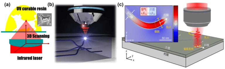
As shown in Figure 1a, the representative method of femtosecond laser additive manufacturing is femtosecond laser two-photon polymerization 3D printing technology. Its basic principle is two-photon absorption and laser focus photopolymerization. Internal modification can create complex micro-nano three-dimensional structures layer by layer. As shown in Figure 1b, the representative method of manufacturing materials such as femtosecond laser is the femtosecond laser-induced change in the internal refractive index of the material. This process does not require material removal. The basic principle is the nonlinear absorption process of the femtosecond laser. inside the hard and brittle material, the representative applications are optical waveguides and fiber networks, etc. As shown in Figure 1c, the representative method of femtosecond laser subtractive material manufacturing is femtosecond laser surface ablation processing and various optional post-processing methods. The extremely high peak power and extremely short pulse time of the femtosecond laser are used to make the material. “Cold” removal is mainly used in the preparation of various functional surfaces as well as in the fields of micro-cutting, micro-drilling and others. Next, the applications of these three types of femtosecond laser processing technologies will be introduced in detail.
Figure 1 Schematic diagram of additive, equal material and subtractive manufacturing with femtosecond laser
Application direction of femtosecond laser treatment
1. Femtosecond laser additive manufacturing and 3D printing by two-photon polymerization
Two-photon polymerization (TPP) is an advanced three-dimensional printing technology at the micro-nano level that uses the two-photon absorption effect to achieve high-precision three-dimensional microstructure fabrication. The basic principle is two-photon absorption and photopolymerization, that is, when the photon density of the ultrafast pulse laser (such as femtosecond laser) is high enough, the molecules of the material can absorb two photons at the same time, and two photons absorption occurs. The two-photon absorption process only occurs at the laser focus, which achieves high spatial selectivity in femtosecond laser processing.
Additionally, during the two-photon absorption process, photoinitiator molecules in the material are excited, triggering a photopolymerization reaction and solidifying the photoresist at the focus by precisely controlling the movement of the laser focus, a complex three-dimensional micro-nano. structures can be built layer by layer. Figure 2 shows the representative nanocow of two-photon polymerization, along with diffractive optical elements such as Fresnel zone plates, refractive optical elements such as compound ocular microlens arrays, microfluidic components, and integrated optics. which can be prepared by this technology. components, etc.
In short, femtosecond laser two-photon polymerization 3D printing technology can be customized according to specific needs and is suitable for the production of small batches, highly complex and personalized products, which is particularly important in medical devices, Custom electronic components and special purpose products. precision parts. This is of great importance in manufacturing.

Figure 2 3D printing by two-photon polymerization (a) nanocow; (b) diffractive optical element (c) refractive optical element (d) integrated optical element;
2. Optical waveguide writing made of femtosecond laser and other materials
With the continuous deepening of social informatization, people’s demand for channel capacity and communication speed is also higher and higher. In order to solve the problem of difficulty in further improving the integration level of traditional electronic chips, researchers proposed the concept of photonic chips with higher stability and faster calculation speed. The femtosecond laser can be used to prepare a real three-dimensional photonic chip inside a hard material. By precisely controlling the femtosecond laser exposure, scan path, and diffuser layout, the most basic unit of the photonic chip, the waveguide, can be controlled. Characteristics such as mode field size, polarization, loss, and single-mode/multi-mode conditions.
Additionally, quantum simulation can be achieved by designing the coupling between different waveguides, and the non-Abelian characteristics of the Sollis photon pump and its interaction with the pump can also be realized by designing waveguide structures. waves with different pump paths in multiple parameter spaces. Wilczek–Zee summation transform associated with the Pu method. As shown in Figure 3a, this is a schematic diagram of spot shape adjustment via a spatial light modulator to prepare a waveguide inside the material. Figures 3b to 3d are respectively a three-dimensional polarization rotator based on direct femtosecond laser writing, with large dimensions. large-scale depth and depth, continuous variable waveguide arrays and integrated photonic chips.

Figure 3 Optical waveguide writing (a) Schematic diagram; (b) Three-dimensional deflection rotator (c) Large-scale and continuous depth-changing waveguide array (d) Integrated photonic chip;
3. Fiber grating writing performed with femtosecond laser and other materials
As an important optical fiber device, fiber network has significant advantages such as anti-electromagnetic interference, low transmission loss, small size, easy reuse and easy integration. It is widely used in fiber sensing, fiber communication, microwave photonics, etc. fields, it has brought landmark revolutions in the fields of optical fiber communications and optical fiber sensing. Therefore, conducting research on the preparation methods and characteristics of fiber gratings will not only help get rid of the dependence on imports of key fiber grating components, but also help accelerate the solution to the “stuck neck” problem in technology and processes. . At the same time, it can also provide strong support and effective guarantee to further promote the maturity, scale and industrialization of fiber network technology in more fields.
Femtosecond laser processing technology provides favorable conditions for the preparation of fiber networks. With the advantages of narrow bandwidth, high energy and high precision of femtosecond laser, the femtosecond laser focused in the fiber core realizes the fiber core through multiphoton absorption. process. Modulating the internal refractive index produces periodic “disturbances” on the light field to obtain fiber gratings, and the process does not need to rely on the photosensitivity of the optical fiber, significantly reducing the complexity of network preparation. In addition, the femtosecond laser can write on different types of fiber materials, including standard single-mode fiber, multi-mode fiber, erbium-doped fiber, etc., which provides flexible options for different application needs and expands its application in detection applications. The fields of communications, lasers and amplifiers have strongly supported the development of optical fiber technology.
As shown in Figure 4, these are sapphire fiber Bragg gratings used for high temperature sensing, point-to-point apodized fiber gratings used in strain sensing, and long-period fiber gratings inscribed by laser-induced refractive index change and sapphire spiral fiber. grids.

Figure 4: writing of the fiber Bragg grating (a) sapphire fiber Bragg grating; (b) spiral fiber network; (c) spiral fiber network;
4. Preparation of functional surfaces by subtractive femtosecond laser manufacturing
The femtosecond laser can realize fine processing at the nanometer level and is suitable for manufacturing high-precision surface micro-nanostructures to customize surface functions. For example, the superhydrophobic and superhydrophilic surfaces shown in Figure 5a are used in the fields of antifouling, anticorrosion and self-cleaning; the anti-reflective and anti-reflective surfaces shown in Figure 5b are used in optical devices, solar cells, aerospace and other fields; The thermally regulated surface shown in Figure 5c for regulating surface heat transfer performance or thermal insulation and the biocompatible surface for biomedical implants and tissue engineering such as cell attachment and growth shown in Figure 5c. Figure 5d.
In short, the application of femtosecond laser in the field of surface micro-nano structure preparation has significantly improved the processing precision and efficiency, expanded the application scope of functional surfaces, and provided solutions for future fields of materials science, optics, electronics and machinery. and biomedicine.

Figure 5 Functional surface (a) superhydrophobic surface (b) antireflective sapphire surface (c) thermoregulated surface (d) biocompatible surface;
5. Multi-material cutting and drilling by subtractive femtosecond laser manufacturing
The application of femtosecond laser in cutting and drilling material surfaces has been widely recognized and applied in many high-tech fields due to its advantages such as high precision, low thermal impact and efficient absorption of energy. For example, in the field of electronic manufacturing, cutting and drilling for chip manufacturing must ensure that the edges of the chip are sharp and free of defects; in the field of medical devices, precision scalpels, micro forceps, etc. are used. for minimally invasive surgical instruments; titanium is used in the aerospace industry Precision cutting and drilling of alloys and composite materials to facilitate the preparation of key components of aircraft and spacecraft; precision processing of turbine blades and engine parts for automobile parts manufacturing to improve processing precision; and efficiency.
In short, the wide application of femtosecond laser in material cutting and drilling gives it huge market potential in high-precision and high-value-added industries such as various communication equipment, precision instruments, new energy batteries and manufacturing of luxury products. The continuous advancement of technology and the expansion of application fields, femtosecond laser will play an important role in more industries. Figure 6a shows the outstanding advantages of femtosecond laser for achieving ultra-stealth cutting in a variety of transparent materials such as glass, semiconductors, laser crystals and ferroelectrics with 10 nm lateral precision and d ‘aspect of 10⁴, and Figure 6b and Figure 6c shows the precision drilling performance obtained on the surface of hard and brittle materials such as sapphire and silicon.

Figure 6 Multi-material cutting and drilling (a) Super invisible cutting; (b) Aluminized sapphire round hole and square hole processing; (c) Silicon wafer group hole processing;
The disruptive ultrafast solution from Jicheng Ultrafast
Jicheng Ultrafast Company has overcome many core technologies that restrict the technical application of ultrafast lasers, including precision processing technology of hard and brittle materials based on laser filamentation and laser modification, optical-mechanical collaborative control technology high precision, laser hull scanning technology, beam stability control technology, error prediction and compensation technology, etc. To overcome the problems of equipment performance improvement research and industrial design, two major categories of femtosecond lasers have been launched Optical processing systems, respectively: 1) Ultra-fast two-photon laser curing 3D printing system of the Maleon series, suitable for applications in micro-optics, microfluidics, integrated photonics, biophotonics, etc. 2) Roban series of femtosecond laser amplifier for micro-nano processing; systems suitable for fiber networks, optical waveguides, precision material surface processing, integrated photonic chips, etc.

Figure 7 (a) Maleon femtosecond laser two-photon polymerization 3D printing system, (b) Roban laser optical waveguide-femtosecond waveguide direct writing system, (c) Writing system Roban-FBG femtosecond laser fiber array, (d) Roban-Nano femtosecond laser processing workstation (supports various deeply customized applications)
Jilin Jicheng Ultrafast Equipment Co., Ltd. was established in 2019 relying on the ultra-fast laser processing team of the State Key Laboratory of Integrated Optoelectronics of Jilin University. The team has accumulated nearly 20 years of femtosecond laser treatment technology. The team’s relevant research results “Fundamental Research on Ultrafast Micro-Nano Laser Preparation of Special Optoelectronic Devices” won the second prize of the National Natural Science Award in 2020; ” won the 2023 National Natural Science Award. Second prize in science.
The company’s micro-nano femtosecond laser processing system has currently filed a number of patents and trademarks for intellectual property protection. The launched femtosecond laser processing system has been used by Tsinghua University, University of Science and Technology of China, Shanghai Jiaotong University, Harbin. Institute of Technology, Nanjing Airlines It is used by dozens of scientific research institutes or enterprise R&D centers such as Aerospace University, Nanjing University of Post and Telecommunications, Anhui University, Guangdong University of Technology, Hebei University, Hebei University of Technology, Huawei Technologies Co.., Ltd., etc.
About the author:
Qi Jinyong, Ph.D., is a process manager at Jilin Jicheng Ultrafast Equipment Co., Ltd., engaged in the research of femtosecond laser processing technology.
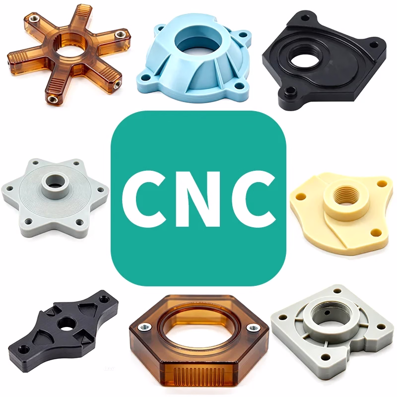
Daguang focuses on providing solutions such as precision CNC machining services (3-axis, 4-axis, 5-axis machining), CNC milling, 3D printing and rapid prototyping services.