3D printing has become an important production tool for high-end applications
Due to technical and financial requirements, the structure of current and future optical instruments in space and aerospace will tend to be highly integrated. The great complexity of the parts makes additive manufacturing(AM) has become a disruptive mode of production. Additionally, as performance requirements increase, optical systems will become increasingly powerful, requiring the development of new manufacturing processes to ensure expected performance. The semiconductor industry is another important area that presents high demands and challenges for ceramic materials.

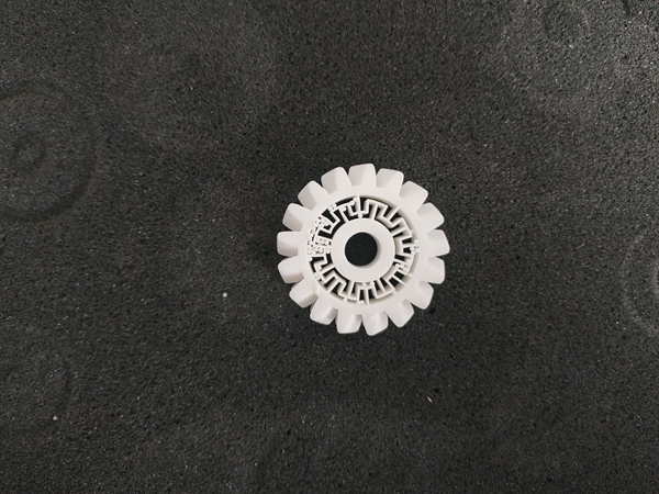
Figure 1 3D printed ceramics
The overall manufacturing process of these products is very demanding, requiring the use of materials with particular chemical, thermal and electronic properties, making ceramic materials the best choice. Additionally, the need for flexible and complex shapes makes3D printing has become a practical solution. Therefore, aerospace and electronics applications will likely be the most important application areas for 3D printed ceramic technology parts over the next 10 years and are expected to reach approximately $764 million by the end of 2030.
The main technical characteristics of optical instruments for space applications are:
• Visual stability
• Resistance to harsh mechanical and thermal environments
• High optical performance as a mission element
Ceramic materials meet these needs thanks to their particular mechanical properties (rigidity, resistance, stability). However, ceramic products are often limited by traditional manufacturing methods, limiting their use to large and small pieces. However, space applications increasingly require optimized large-scale optical instruments. For example, satellite mirrors must be as light as possible. Only additive manufacturing can optimize the design and production of these new mirrors.

To meet growing demand,3Dceram has developed the C3600 Ultimate 3D printer, which has a 600mm x 600mm x 300mm (length x width x height) printing platform, making it its largest stereolithography printer.

to useThe C3600 Ultimate 3D printer offers many advantages for producing optical parts, such as:
• Shortened lead times: The traditional manufacturing process for optical parts includes 6 stages (production of blanks – lightening by machining – grinding – polishing – coating – surface integration). 3D printing can avoid machining and grinding steps
• Ceramic material savings: Typically 90% of the blank weight is removed by machining, leading to excess scrap and a high risk of cracking.
• Disruptive design: more complex designs and weight reduction designs can be considered
• Functional integration: such as internal channels, electrical traces and power supplies
• Print large parts: Figure 2


picture2: The satellite mirror with a diameter of 500mm adopts a closed structure and can be printed on a C3600 printer in less than 1 day.
The 3DCERAM process can simplify and reduce the manufacturing process. This opens a new avenue for the development of cooled optical systems, active optical systems or free-form optical systems. The forming function of 3D printing also improves the quality of the integration/bonding process with higher precision. Thus, with the CERAMAKER C3600 printer, it is now possible to produce large “custom” ceramic optical substrates, thereby reducing risks in the manufacturing process. Additionally, new mirror designs also include the exploration of semi-closed structures and integrated interfaces that can reduce weight (Figure 2).
The 3DCERAM process also opens up new perspectives for new generation instruments:
• Compact solutions with integrated functions (thermal insulators, cooling channels, etc.)
• Limits of mechanical and thermal interfaces
• Integrate optical functions into structural devices
The 3DCERAM C3600 Ultimate printer is now capable of producing a range of large and complex optical substrates or structural parts in the aerospace industry, suitable for the most challenging environments.
electricity child answer to use
In recent years, semiconductor manufacturing plants have developed increasingly complex processes that require special equipment to meet their needs. Additionally, growing market demand for microcircuit capacity has led to increasing use of diameterssilicon wafers from 1 to 12 inches (25 to 300 mm) and develop equipment to process them to obtain the required deposits.
To better understand the role of ceramic materials in the semiconductor industry, here is a brief introduction to the main steps involved in the manufacturing of integrated circuit chips:
• Wafer processing is carried out by cutting single crystal pillars of silicon or gallium arsenide to obtain round wafers.
• The oxidation process is a necessary step to form a protective film on the wafer surface.
• The photolithography process is used to “print” circuit patterns onto wafers.
• The etching process removes excess oxide film, leaving only the semiconductor circuit diagram.
• Thin film deposition is used to create a multilayer structure composed of alternating conductive and insulating films on the wafer surface.
• The interconnection process allows the transmission of energy and signals.
• Assembly, packaging and final testing
All these steps are aimed at extending the life of equipment and reducing operating costs. Besides the need to work in extremely clean conditions, the different deposition techniques used, e.g.CVD, PECVD, ALD; materials with specific properties are also necessary to obtain and maintain the perfect conditions required to manufacture these high-performance products.
Among the ceramic materials, the most demanded are:
• Common oxides: such as alumina, zirconia, silica, cordierite, which represent the majority of the market but there are also oxides with higher added value: such as yttrium trioxide;
• Nitride: aluminum nitride and silicon nitride
• Carbide: silicon carbide
Here are some examples of ceramic parts used in the semiconductor industry:

picture3: Printing time for this large part on the CERAMAKER C3600 printer was 21 hours and 49 minutes
• In the wafer cleaning stage, ceramic materials are used in the wafer transfer plate, chuck/suction cup (Figure 3), and robot arm.
• In thermal diffusion and chemical vapor deposition processes, many components such as radiant tubes, wafer vessels, and gas inlets are made of ceramic.
• Ceramics are used in chambers, electrostatic chucks, nozzles and rings during plasma etching.
• Ceramic can also be used as a heating element during heat treatment
Also,The 3D printing process appears to be a promising technological option for the production of these high-tech parts due to its flexibility and responsiveness, as well as the feasibility of printing complex geometries.
In 2018, Alumina Systems Co., Ltd. has achieved great success in the semiconductor industry through ceramic 3D printing. The company received the Best Component Award from CERAMITEC Munich/Germany for the development of a 380 mm diameter ceramic gas distribution ring for the PEALD (Plasma Enhanced Atomic Layer Deposition) process. Thanks to its clever geometry, the ring can deliver two gases simultaneously or sequentially. PEALD is an innovative process suitable for the production of semiconductors, presenting significant technological improvement and presenting enormous economic potential.
total Node
Additive manufacturing brings new possibilities to the industrial production process of optical and semiconductor instruments. In addition to saving time and reducing material loss, the technology also has the following advantages:
• Create revolutionary designs
• Improved stiffness/mass ratio
• New features such as integrated cooling channels or thermal insulators
• Simplify and optimize the design process
Of all the additive manufacturing processes, stereolithography has emerged as the most suitable for these applications, because it allows optimized results in terms of print quality, spatial resolution and material properties. In order to improve its performance and its lifespan, future semiconductors/ Manufacturing processes for optical products will become faster and even more radical. Well, the combination of specific ceramic materials and the commercialization of industrial 3D printers are essential assets to meet future challenges in these areas.
This article is taken from: “CERAMICS APPLICATIONS” in October 2022
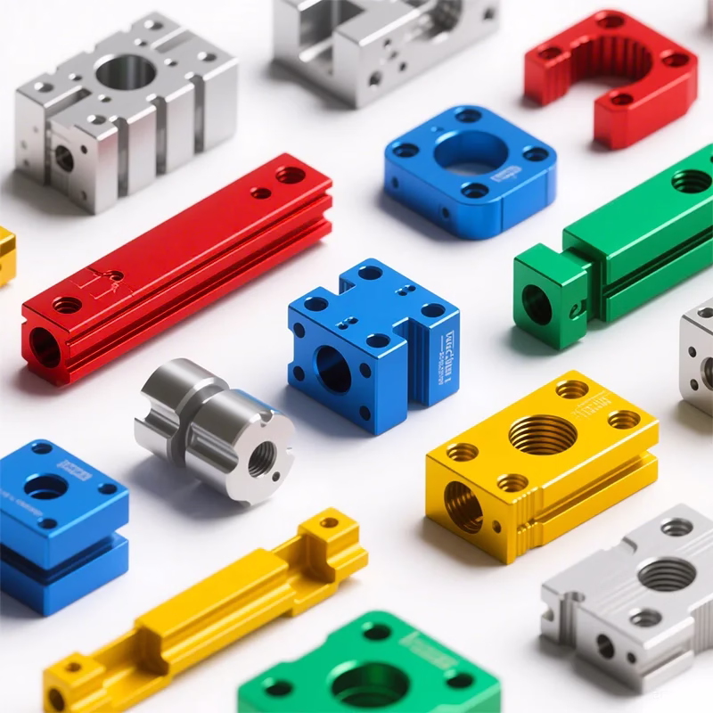
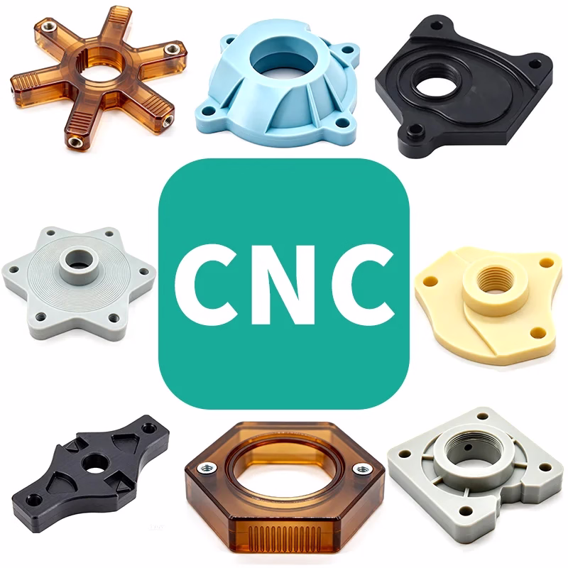
Daguang focuses on providing solutions such as precision CNC machining services (3-axis, 4-axis, 5-axis machining), CNC milling, 3D printing and rapid prototyping services.