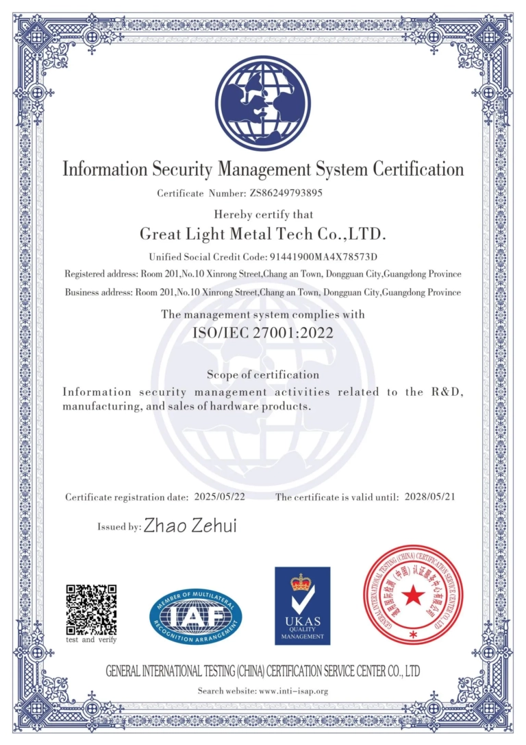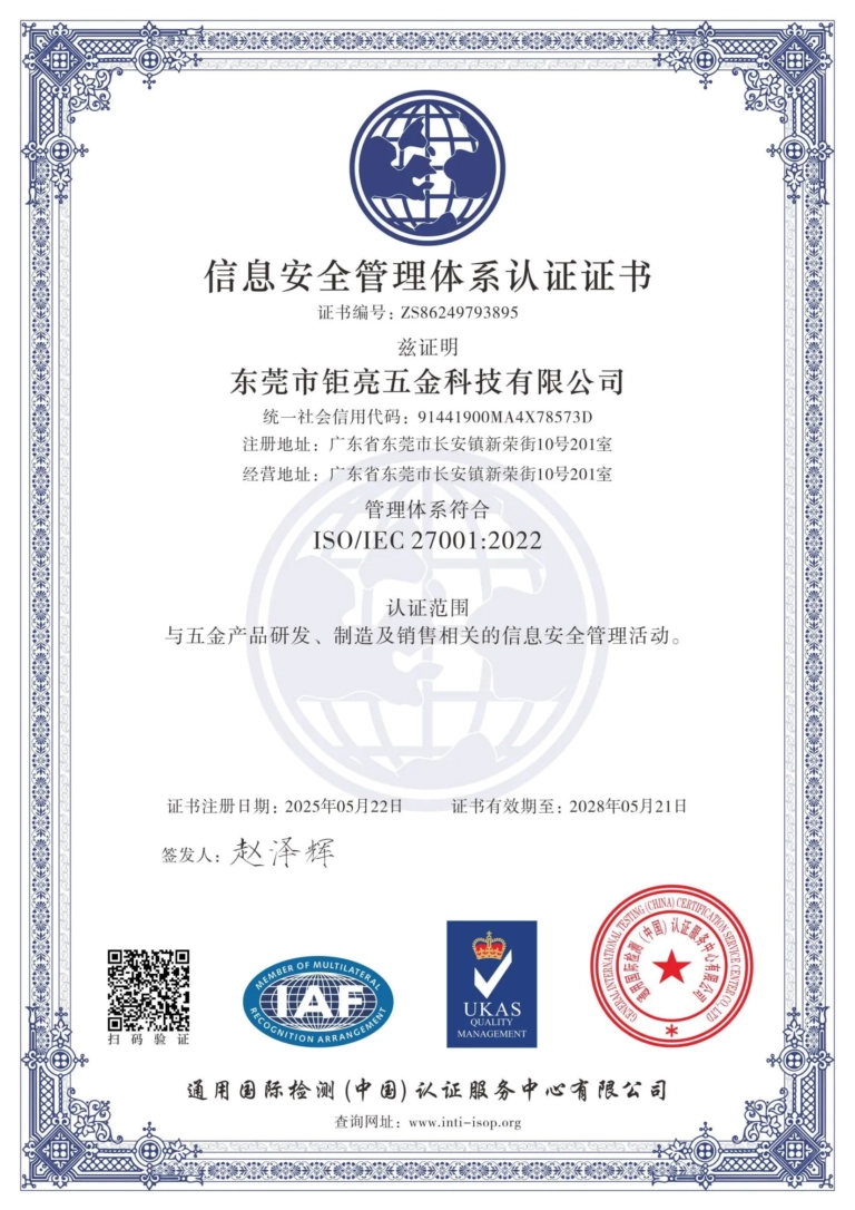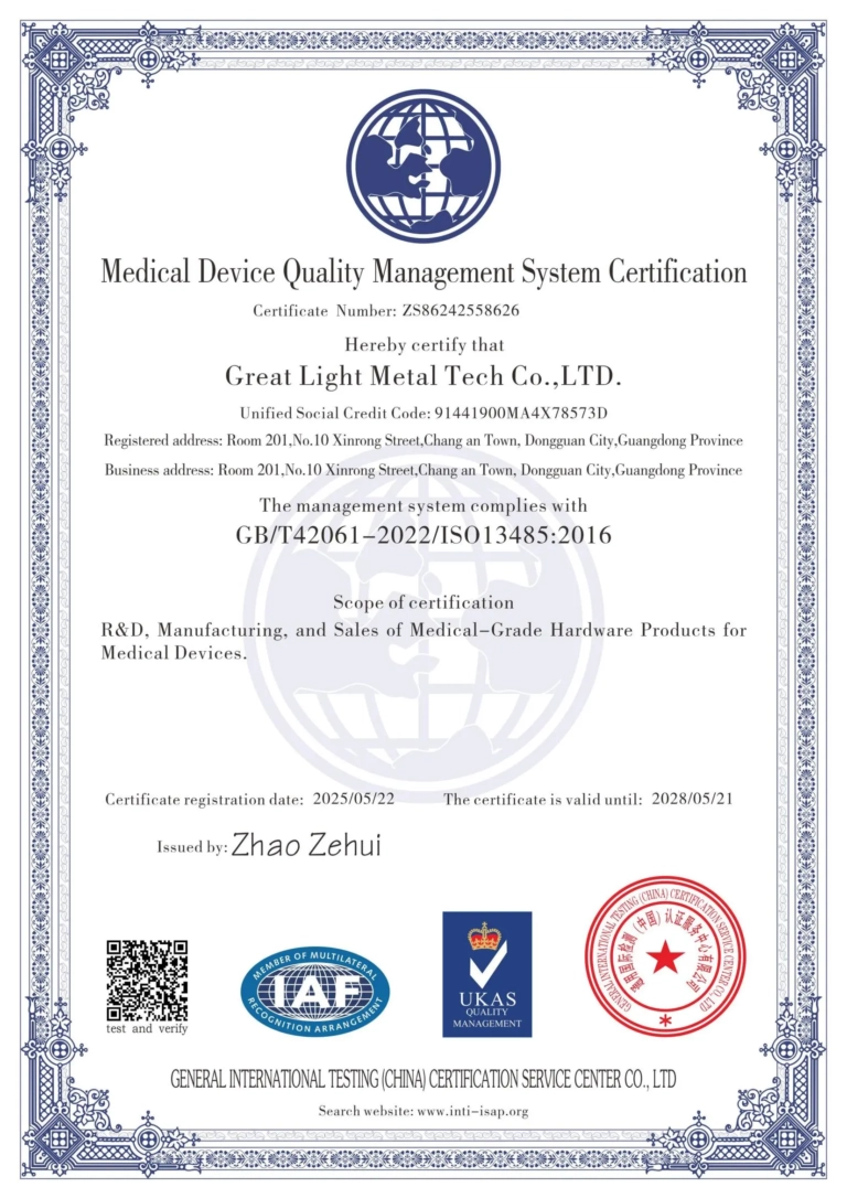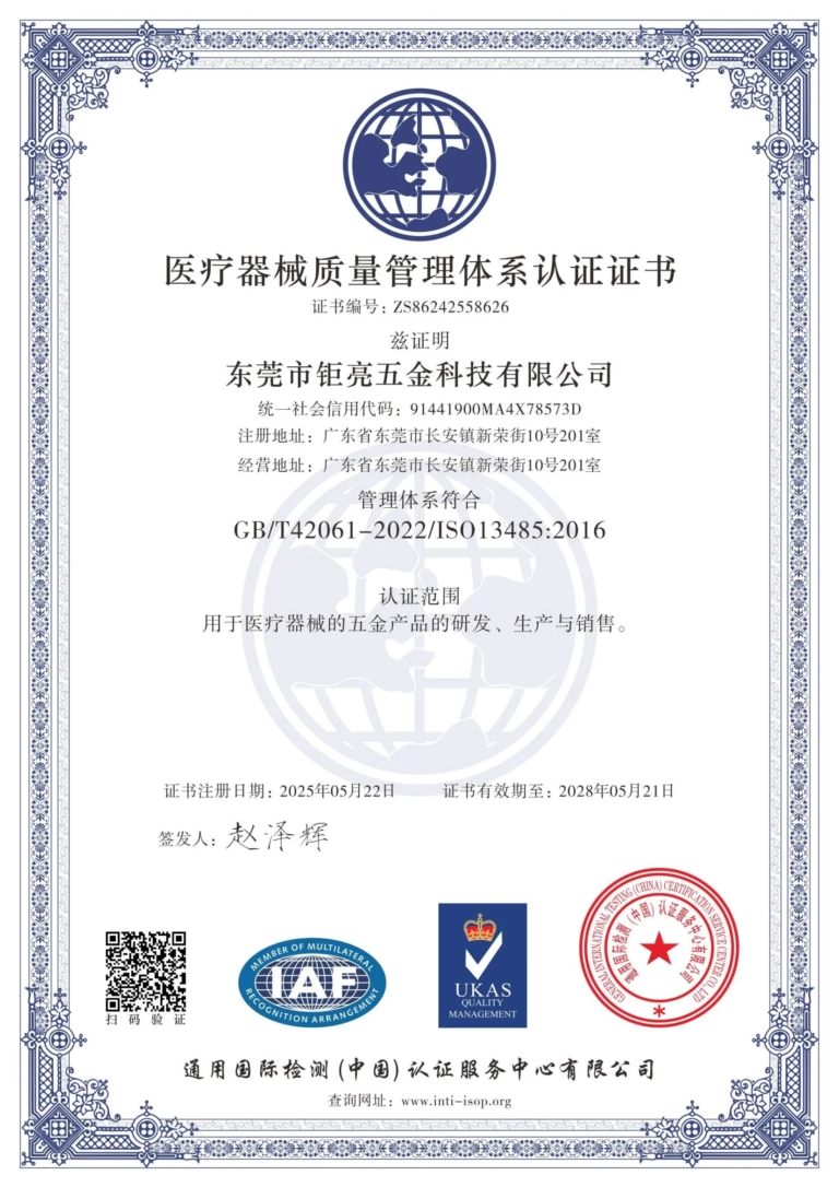
According to Memes Consulting, recently the Karlsruhe Institute of Technology in Germany (Karlsruhe Institute of Technology)KIT) developed a new type of3DThe printing process produces nano-thin quartz glass structures printed directly on semiconductor chips.

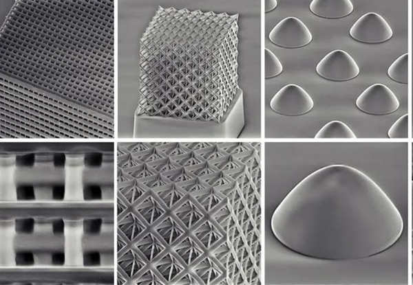
△New type3DPrinting process results in a wide variety of nanoscale quartz glass structures
organic–Inorganic hybrid polymer resin used as silica3DStarting material for printing. As this process does not require sintering, the temperatures required are much lower. At the same time, higher resolution enables nanophotonics for visible light. This research work is inSciencereported in the journal.
Nanofine quartz glass structures composed of pure silica3DPrinting opens up new possibilities for numerous applications in optics, photonics and semiconductor technology. However, until now, processes based on conventional sintered silica have dominated.
The temperatures required to sinter silica nanoparticles exceed1100Celsius – too high for direct deposition on semiconductor chips. by the Institute of Nanotechnology at the Karlsruhe Institute of Technology (INT)Jens BauerA PhD-led research team has now developed a new process capable of producing visible-light transparent quartz glass with high resolution and excellent mechanical properties at significantly reduced temperatures.
Jens BauerKarlsruhe Institute of TechnologyEmmy NoetherThe research group “Nanostructured metamaterials (Nanoarchitectural metamaterials)”, he and the University of California at Irvine (the University of California at Irvine) and Irvine Medical Technologies, Inc.Edwards Life Sciencescolleagues inScienceThe magazine presents this news3DPrinting process.
A specially developed organic product–Inorganic hybrid polymer resins are used as raw materials, consisting of polyhedral oligomeric silsesquioxane molecules (POSSIBLE) Composition: Tiny cage-shaped silica molecules with organic functional groups.
Once formed, it will be completely3DThe printed and networked nanostructures were heated in air to650temperature in degrees Celsius. During this process, organic components are expelled while inorganic componentsPOSSIBLEThe cages combine to form continuous fused silica microstructures or nanostructures. The process requires only half the temperature of nanoparticle-based sintering processes.
Jens Bauerexplains: “The lower temperatures enable the printing of robust, transparent, free-form optical glass structures directly on semiconductor chips at the resolution required for visible light nanophotonics. In addition to the excellent optical quality, the quartz produced by this process also has excellent mechanical properties and is easy to process.
Used by research teamsPOSSIBLEThe resin prints many different nanoscale structures, including97Photonic crystals for nanobeams, parabolic microlenses, microlenses with nanostructures. “OUR3DThe printing process allows the structure to withstand harsh chemical or thermal conditions. “Jens Baueradded.
Depend onJens BauerThe research team led by3D material made to order(3DMM2O) center of excellence – these are the Karlsruhe Institute of Technology and the University of Heidelberg (University of Heidelberg), which embodies the combination of natural sciences and engineering sciences, a highly interdisciplinary research approach.Jens BauerThe goal is to3DAdditive manufacturing processes are taken to the next level.
source:MEMS
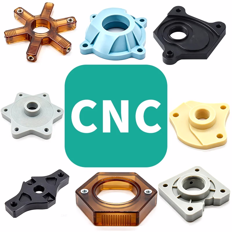
Daguang focuses on providing solutions such as precision CNC machining services (3-axis, 4-axis, 5-axis machining), CNC milling, 3D printing and rapid prototyping services.