A wafer must undergo three changes before it can become a real semiconductor chip: first, the block-shaped ingot is sliced; In the second process, the front side of the wafer is cut according to the previous process. The transistors are etched. Finally, the wafer is packaged, which is a cutting process that turns the wafer into a complete semiconductor chip. It can be seen that the packaging process is a back-end process. In this process, the wafer will be cut into individual chips of hexahedral shape. This process of obtaining independent chips is called “Singulaton”, and the wafer will be cut into. individual chips. The process of sawing a circular plate into independent rectangular parallelepipeds is called “die sawing”. Recently, with the improvement of semiconductor integration, the thickness of wafers has become thinner, which of course brings a lot of difficulty to the “one-off” process.
The history of the development of wafer cutting
The front-end and back-end processes further evolve by interacting in various ways: The evolution of the back-end process can determine the structure and position of the hexahedral chiplets on the wafer (individually separated chip), as well as on the wafer. pads (electrical connection paths); Rather, the evolution of the front-end process has changed the process and method of thinning the backside of wafers and “pressure sawing” wafers in the back-end process. Therefore, the appearance of the package becomes more and more sophisticated, which will have a big impact on the back-end process. In addition, depending on the change in packaging appearance, the number of cuts, procedures and types will also change accordingly.
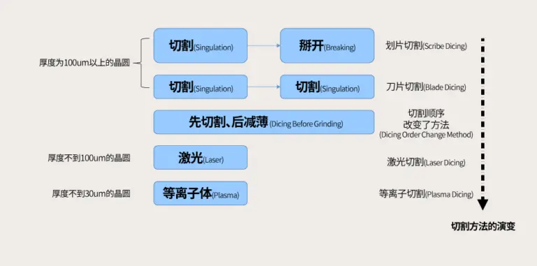
Scribe cutting

Initially, “breaking” by applying an external force was the only cutting method to divide the wafer into hexagonal dies. However, this method has disadvantages such as chipping or cracking at the chip edge. In addition, because the burrs (Burr: some residue produced during cutting) are not completely removed from the metal surface, the cut surface is also very rough.
In order to solve this problem, the cutting method “Scribing” was created, i.e. the surface of the wafer is cut to approximately half the depth before “breaking”. “Dicing,” as the name suggests, refers to the use of a turbine to pre-saw (half-cut) the front face of the wafer. At first, most wafers smaller than 6 inches used this cutting method of first “dicing” and then “breaking” between the chips.
Dicing or sawing with a blade

The “dicing” cutting method gradually developed into the “blade dicing” cutting (or sawing) method, which is a cutting method using a blade two or three times in succession. The “blade” cutting method can compensate for the peeling of small chips during “breaking” after “slicing” and can protect small chips during the “singling” process. “Blade” cutting is different from the previous “slicing” cutting, that is, after making a “blade” cut, it is not “broken”, but is cut again with the blade. This is why it is also called the “Step Dicing” method.

To protect the wafer from external damage during the cutting process, an adhesive film is applied to the wafer in advance to ensure safer “cutting”. During the “Back Grinding” process, the adhesive film is attached to the front face of the wafer. On the other hand, in “blade” dicing, the adhesive film is applied to the back side of the wafer. During the process of chip eutectic bonding (fixing separate chips to the PCB or rack), the adhesive film on the back of the chip will fall off automatically. Due to the high friction when cutting, DI water must be sprayed continuously in all directions. In addition, the wheel must be equipped with diamond particles in order to slice it better. At this stage, the cut (blade thickness: groove width) must be even and must not exceed the width of the scribing groove. For a long time, sawing was the most widely used traditional cutting method. Its biggest advantage is that it allows a large number of wafers to be cut in a short time. However, if the wafer feed speed is significantly increased, the possibility of peeling off the edges of small chips will increase. Therefore, the number of revolutions of the turbine must be controlled at approximately 30,000 times per minute. It can be seen that semiconductor technology is often a secret accumulated slowly over a long period of accumulation and trial and error.
Dicing Before Grinding (DBG): Cutting order changes method

When you perform blade dicing on 8-inch diameter slices, you don’t have to worry about chip edge peeling or cracking. But as the wafer diameter increased to 21 inches and the thickness became extremely thin, peeling and cracking began to appear again. To significantly reduce the physical impact on the wafer during the cutting process, the DBG method of “cut first, grind later” replaces the traditional cutting sequence. Different from the traditional “blade” cutting method which performs continuous cutting, DBG first performs “blade” cutting, then gradually thins the wafer through continuous thinning from the back until the chip divides. It can be said that DBG is an improved version of the previous “blade” cutting method. Because it can reduce the impact of the second cut, the DBG method was quickly popularized in “slice-level packaging”.
Laser cutting

The Wafer Level Chip Scale Package (WLCSP) process primarily uses laser cutting. Using laser cutting can reduce peeling and cracking, thereby obtaining higher quality chips, but when the wafer thickness is greater than 100 μm, productivity will be significantly reduced. Therefore, it is mainly used on wafers with a thickness of less than 100 μm (relatively thin). Laser cutting cuts silicon by applying high-energy laser light to the cutting grooves of the wafer. However, when using the Conventional Laser cutting method, a protective film must first be applied to the wafer surface. Because when the wafer surface is heated or laser irradiated, these physical contacts will produce grooves on the wafer surface and the cut silicon fragments will also adhere to the surface. It can be seen that the traditional laser cutting method also directly cuts the surface of the wafer, in this respect it is similar to the “blade” cutting method.
Stealth Dicing (SD) is a method that first uses laser energy to cut the inside of the wafer, then applies external pressure to the strip attached to the back to break it and separate it. the chip. When pressure is applied to the ribbon on the back, the wafer will be momentarily lifted upwards due to the stretching of the ribbon, causing the chips to separate. Compared with the traditional SD laser cutting method, the advantages are: firstly, there is no silicon scrap; second, the incision (Kerf: the width of the scribing groove) is narrow, which allows more chips to be obtained. Additionally, peeling and cracking will also be significantly reduced using the SD method, which is essential in determining the overall quality of the cut. Therefore, SD method is expected to become the most popular technology in the future.
Plasma cutting
Plasma cutting is a recently developed technology that uses plasma etching for cutting during the manufacturing (Fab) process. Plasma cutting uses semi-gaseous materials instead of liquids, so it has relatively little impact on the environment. In addition, the whole slice cutting method at one time is adopted, so the “cutting” speed is relatively fast. However, the plasma method uses chemical reaction gas as raw material, and the etching process is very complicated, so its operation is relatively tedious. However, compared to “blade” cutting and laser cutting, plasma cutting does not damage the wafer surface, thereby reducing the defect rate and obtaining more chips.
Recently, as the wafer thickness has been reduced to 30 μm, many materials such as copper (Cu) or low dielectric constant (Low-k) are used. Thus, in order to avoid burrs, plasma cutting methods will also be favored. Of course, plasma cutting technology is also constantly evolving. I think that in the near future it will no longer be necessary to wear a special mask when engraving, because this is a major development direction in plasma cutting.
As wafer thickness continues to thin, from 100 μm to 50 μm, then to 30 μm, cutting methods to obtain independent chips have also evolved from “snap”, “blade” cutting, to laser cutting, then plasma. Changes are developing. Although increasingly mature cutting methods have led to an increase in the production cost of the cutting process itself, significantly reducing peeling, cracking and other undesirable phenomena that often occur when cutting semi-finished chips. -conductive and increasing the number of chips obtained per wafer unit, the production cost of a single chip showed a downward trend. Of course, the increase in the number of chips obtained per unit surface of the wafer is closely linked to the reduction in the width of the cutting groove (Dicing Street width). Using plasma cutting method, compared with “blade” cutting method, almost 20% more chips can be obtained, which is also one of the main reasons why people choose the method plasma cutting. With the development and changes of wafers, chip appearance and packaging methods, various cutting processes such as wafer processing technology and DBG are also emerging.
Daguang focuses on providing solutions such as precision CNC machining services (3-axis, 4-axis, 5-axis machining), CNC milling, 3D printing and rapid prototyping services.