1 Introduction
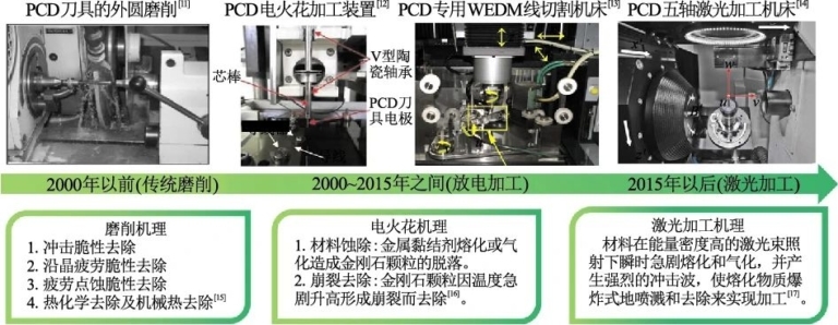
PCD cutting tools are one of the main tools for processing hard and brittle materials (graphite, glass, etc.) with high efficiency and quality. Commonly used PCD tool processing methods include grinding and grinding, electrical discharge machining, laser processing, etc. Figure 1 lists the main processing methods, removal mechanisms and processing equipment of PCD tools. Among them, grinding and abrasive processing have the problem of large grinding force, which will cause defects such as cracks, local fractures and graphitization on the processed surface, the thermal effect of EDM will affect the geometric precision of the tool and micro-; cracks may exist on the cutting edge. Affects the mechanical properties of the tool. Additionally, there are composite processing methods aided by technologies such as ultrasound, ion beam, chemistry, and discharge. Among them, ultrasonic processing has problems such as high consumption of diamond powder, significant dust pollution and damage to workers’ health; Ion beam processing involves complex operations, expensive equipment, and extremely low material removal rate, which makes industrialization difficult. The above methods all have low processing efficiency and certain processing limitations.
Laser processing has the advantages of high efficiency, high precision and low material damage, which can avoid potential problems in traditional processes when processing PCD tools. At the same time, laser processing also has the characteristics of adjustable energy, no noise and flexible processing methods, which greatly reduces the application limits. Therefore, in the field of precision processing of diamond and hard and brittle materials, laser and laser. Composite preparation methods will become increasingly common. However, laser processing presents problems such as micrographitization of the treated surface. Many domestic and foreign researchers have carried out in-depth research on the removal mechanism of PCD materials during laser processing and the laser-induced graphitization process.
Figure 1 Development process of traditional PCD tool processing technology
This article focuses on the removal mechanism of PCD materials in laser processing, summarizes the influence of process parameters such as wavelength and pulse width on the processing quality in laser material processing PCD and comparatively analyzes the process technology and processing performance of various types of PCD. laser processing tools at home and abroad. The research and development progress and current situation of domestic laser processing equipment are introduced. This will help promote the application of PCD tool processing technology and provide technical support and references for the development and technical application of PCD tool laser processing technology.
2 Laser processing mechanism and PCD material processing methods
2.1 Mechanism of laser removal of PCD materials
The diamond removal mechanism in laser processing of PCD materials mainly includes chemical removal and vaporization removal. During laser processing, laser photons directly destroy the diamond bond and convert diamond particles into graphite phase. When the temperature approaches or exceeds the graphitization temperature (700°C), the graphite reacts chemically with oxygen in the air to produce CO2 and CO. for volatile gases, this will The method of removing material is called chemical removal. Therefore, the chemical removal rate of diamond is closely related to the oxygen concentration in the air; when the laser energy density is high enough, the surface graphite will reach a sublimation temperature of 4000°C. °C, and the graphite is removed in the form of sublimation. This method of disposal is called gasification disposal. With the increase of laser energy density, the removal mechanism of diamond particles gradually changes from chemical removal of graphite phase to gasification removal. The gasification removal rate is determined by the energy density of the laser. Since the thermal conductivity of diamond is much higher than that of metal binders such as cobalt, heat will be quickly conducted to the surrounding diamond materials, causing the temperature to rise rapidly. However, cobalt has low thermal conductivity and a slow thermal radiation transfer rate. Heat is concentrated in the top layer of the cobalt material and is difficult to diffuse to surrounding materials, so diamond particles are easier to remove than cobalt. The cobalt layer agglomerated on the surface after laser ablation can be removed by pickling, etc., and the remaining graphite debris can be removed by soaking in organic solvents (ethanol, methanol or acetone, etc.), acidic detergents or ultrasonic cleaning.
During the laser removal process of PCD material, the specific graphitization process is shown in Figure 2. Under multi-pulse and high heat flux laser irradiation, the diamond transforms into amorphous carbon, from the arrangement Initial sp3 hybrid of diamond molecules (see Figure 3b). ). After further irradiation, the sp2 structure will transform again into an sp3 hybrid arrangement, becoming “diamond-like”. The phenomenon of diamond graphitization can be confirmed by identifying the multilayer graphitic carbon structure through techniques such as Raman spectroscopy, scanning electron microscopy, and transmission electron microscopy. Depending on the interaction time between the laser and the material, the graphitization process can be confirmed. interrupted and only high orientation is formed of graphite without formation of amorphous carbon. Strekalov V. et al. described the crystal nucleation mechanism during laser-induced graphitization. The diamond particles in the laser-focused point irradiation zone will form nucleation of “tiny graphite droplets” on the nanoscale. As the “graphite droplets” grow and fall, mechanical stress and mechanical damage occur in these areas and new defect sites are generated. New graphitic carbon crystals nucleate and grow at the newly formed defect sites. Since PCD materials are composed of diamond and metal binders, they have defect sites (such as impurities, gaps, and microcracks). These defects can also provide sites for crystal nucleation and growth. Kuznetsov VL et al. summarized the chain catalytic graphitization mechanism used to describe the transformation of diamond into graphitic carbon crystals and the catalytic mechanism of metal binders such as cobalt affecting the graphitization process. Diamond first undergoes chain decomposition of its atomic structure to generate graphene crystals, and then graphitic carbon crystals diffuse into cobalt to form a cobalt-carbon solid solution. As the temperature continues to increase, the cobalt melts, fragments, and fragments. migrates from the crystal structure, carbon precipitates as graphitic carbon crystals, forming polycrystalline graphite. Additionally, the melting temperature of binders such as cobalt is lower than that of diamond, so the liquid phase is dispersed into the grain structure earlier during the laser ablation process and the structure will not recover after cooling. In addition, the thermal expansion coefficients of the binder and the diamond are different, and the microcracks caused by residual stresses after cooling will reduce the fatigue life of the material.

Figure 2 Graphitization process of a diamond crystal under conditions of strong multi-pulse laser irradiation

Figure 3 Different types of hybridization
The interaction time between the laser and the material is affected by the energy density of the laser and the pulse duration. In the laser processing process of PCD materials, the thickness of the diamond graphitization layer on the material surface is determined by the relationship between the laser input energy and the ablation threshold of the material. When the energy density is below the ablation threshold, laser irradiation only causes a phase change within the material and then leads to graphitization. As the energy density increases, the degree of graphitization becomes more intense when the energy density is above the ablation threshold; , a macroscopic graphitization phenomenon was observed, and as the laser energy became denser As the intensity increases, the graphite layer formed on the surface will be further ablated, leaving more obvious ablation pits; between nanoseconds and microseconds, as the pulse width increases, the thickness of the heat affected zone will increase significantly, which will also increase. leads to an increase in the ablation threshold, thus reducing the graphitization rate.
The heat-affected zone (HAZ) and graphitization thickness caused by different pulse widths are shown in Figure 4. The heating time of the long-pulse laser is long, and the irradiation heat is dispersed in a small range, so the temperature is not high. , which is not conducive to the graphitization phase transformation of diamond. The pulse duration of nanosecond lasers is longer than that of picosecond lasers and the risk of thermally induced phase changes is relatively low, but a small graphitization process will still occur due to overheating of the local area when l laser interaction. Between nanosecond and femtosecond pulse widths, as the pulse width decreases, the thickness of the graphite layer also decreases. The femtosecond laser has almost no heat-affected zone, so the thickness of the graphite layer is only in the nanometer range.

Figure 4 Effect of pulse duration on thermal transition of laser-processed PCD
Additionally, when other parameters are constant, decreasing the laser scanning speed increases the number of pulses irradiating a fixed position per unit time, resulting in a decrease in the ablation threshold, the energy density will be higher than the ablation threshold, the graphitization rate will increase and the thickness of the graphite layer will decrease; when the power increases or the repetition frequency decreases, the increase in energy density will also cause the degree of graphitization to increase. The graphitization phase transformation of diamond will reduce the surface hardness of diamond material, thereby reducing the difficulty of subsequent mechanical removal during laser-mechanical composite processing.
Eberle G. et al. summarized the removal mechanism of PCD material and thermal damage by different pulse-width lasers from the perspective of thermal coupling between electrons and crystal lattice (see Figure 5). Since PCD materials are extremely hard materials with low thermal expansion coefficients, the electronic relaxation time of PCD is generally a few picoseconds, and the energy conduction will be limited to the optical penetration depth, not the depth thermal, and generally does not modify the surrounding area. the microstructure of the material to be treated. However, a shorter pulse duration will also cause a certain degree of thermal damage, and when the temperature of the electrons and lattice under the action of the laser is higher than the starting temperature of graphitization, there is a certain probability that ‘graphitization occurs. The duration of the femtosecond pulse is less than the relaxation time of the electron, there is no thermal coupling between the electron and the crystal lattice, and the extremely high peak power induces nonlinear multiphoton absorption, which undergoes tunnel ionization (usually after 1 fs), avalanche ionization (about after 50fs), electronic heating (after about 100 fs) and other phenomena, the main elimination mechanism is the breakdown of bonding and phase explosion, causing the material to be ejected at a speed of up to 102 ~ 103 m/s. There is almost no heat affected area and is smooth. , uniform and clear texture contours can be processed. The picosecond pulse duration is close to the electron relaxation time, and the pulse duration and lattice heating time are at the threshold, so the electrons have time to reach thermal equilibrium with the network thanks to the conduction of thermal energy. by phase explosion, boiling, phase separation and gas. The material is ejected at a speed of 102 m/s, the heat affected zone is small, and the risk of thermally induced defects such as melt fragments and graphitization is reduced. The pulse duration in nanoseconds is longer than the network heating time. There is a direct thermal coupling between the electrons and the lattice. Removal of materials relies on heating, melting and evaporation. The heat-affected zone is a form of allotropic carbon transformation, melting, and recrystallization. The shaped carbon layer can easily cause streaks on the material after processing. The microsecond level pulse laser uses the energy obtained by linear absorption of electronic resonance in PCD materials to gradually melt and evaporate the material. The heat affected zone is large and can easily cause thermal damage to materials such as cracking. used to reduce thermal damage. Use less frequently.

Figure 5 Comparison of the effects of different pulsed lasers on PCD materials
Based on the above research, the removal mechanism of PCD materials under laser irradiation is mainly diamond graphitization and laser-induced material removal, including chemical removal and vaporization removal. When the processing temperature reaches the graphite sublimation temperature, the chemical removal changes to vaporization removal. The degree of graphitization on the surface of PCD material processing is affected by the laser energy density and laser pulse duration. An increase in laser energy density will result in an increase in the degree of graphitization. Between nanosecond and microsecond pulse widths, increasing the pulse width is beneficial to reduce the degree of graphitization; Between nanosecond and femtosecond pulse widths, reducing the pulse width is beneficial to reduce the thickness of the graphite layer. In addition, by comparing the pulse duration and electron relaxation time, the thermal damage and graphitization of PCD material during laser irradiation can be analyzed from the perspective of the thermal coupling relationship between electrons. and the crystal lattice.
2.2 The influence of laser process parameters on the quality of PCD processing
2.2.1 Wavelength
The absorption rate of laser energy by PCD materials is affected by the laser wavelength. The shorter the wavelength, the photon energy corresponding to the wavelength of 1064 nm is 1170 meV and the photon energy corresponding to the wavelength of 532 nm is 2330 meV. For PCD materials, the binding energy of the carbon-carbon (CC) single bond is 347meV. The photon energy of 1170meV is higher than the bond energy of the PCD material, which is sufficient to destroy the material’s molecular bonds, hence shorter. laser wavelengths have higher photon wear efficiency. When laser processing PCD materials, in order to achieve better ablation rate and processing precision, an infrared laser with a wavelength of about 1064 nm or a green laser with a wavelength 532 nm waveform is generally used. Zhang G. et al. compared the effects of lasers at different wavelengths on cutting PCD composite wafers and found that the 1064 nm Nd:YAG laser caused the formation of periodic bands on the cutting surface, while the KTP/ Nd:YAG at 532 nm had no streaks. . Éberlé G. et al. studied the effects of two wavelengths (532 nm and 1064 nm) and two pulse widths (1 ns and 10 ps) on laser processing of PCD. Under both pulse widths, the 532 nm wavelength exhibits higher material removal than the 1064 nm wavelength. for the 1 ns pulse width laser, the wavelength of 532 nm has lower surface roughness, and as the 10 ps pulse width laser has a high material removal rate and can clean the surface of PCD material, the surface roughness of the two wavelengths is basically the same. The same.
2.2.2 Pulse width setting
The deposition and distribution of energy on the PCD material irradiated by laser irradiation with different pulse widths will also affect the energy absorption of PCD. Since the heat-affected zone of the continuous laser is too large and has little research value, it will not be discussed here. The heat-affected zone of pulsed laser will become smaller as the pulse width decreases, making it suitable for processing PCD materials. The pulse duration has a significant impact on the photon absorption of the material. From microsecond laser to femtosecond laser, the absorption of photon energy gradually changes from linear absorption to nonlinear absorption (multiphoton absorption), which has a significant impact on the treatment effect.
In order to study the impact of laser processing of PCD materials with different pulse widths, Eberle G. et al. used lasers with pulse durations ranging from long microseconds to ultra-short picoseconds to process PCD materials and compared the thickness of the graphitic carbon layer. and the size of the heat-affected zone of different pulse lasers (see Figure 6), research shows that compared to microsecond pulses and nanosecond pulses, picosecond pulses do not have a significant heat-affected zone or layer of residual graphite, and have a higher ablation. rate and lower surface roughness. Okuchi T. et al. used nanosecond near-infrared lasers and femtosecond near-infrared lasers to process ultra-hard nanopolycrystalline diamond (Nano-PCD). Research shows that near-infrared nanosecond lasers are suitable for rapid prototyping and surface deformation is high. about 10 μm and there is a graphite layer, while the near-infrared femtosecond laser is suitable for precision micro-machining and surface treatment. It can produce a submicron smooth surface without graphite layer, but the material removal efficiency is the lowest. Chang FY et al. analyzed the influence of different pulse widths on the surface morphology of PCD blank processing. Research has shown that incision depth increases with increasing pulse width. In summary, the smaller the pulse width, the higher the processing precision, the lower the processing efficiency, and the lower the degree of graphitization.

(a) Microsecond laser

(b) Nanosecond laser

(c) Picosecond laser
Figure 6 Cross sections of laser-processed PCD materials with different pulse widths
2.2.3 Other process parameters
Laser processing is also affected by factors such as laser energy density, dot overlap rate, degree of defocus and scanning speed. Su Y. et al. found that the higher the average power, the more the PCD removal depth and width and surface roughness increased, the removal depth and width showed a decreasing trend; the amount of defocus increases With the increase, the spot becomes larger, the laser energy density decreases, the removal depth becomes shallower, and the precision decreases. Wu Q. used a nanosecond laser to process PCD materials and found that the surface roughness and material removal rate increased with increasing laser energy density. The impact of pulse overlap ratio on surface roughness is relatively small. Continually increasing the pulse overlap rate (>95%) will result in a marginal decrease in the material removal rate. Higher PCD can be achieved with appropriate pulse overlap. (<95%), removal rate and reduction of surface roughness and underground damage. In addition, the scan overlap rate has a relatively large impact on the surface roughness. As the scan overlap rate increases, the material removal rate shows a decreasing trend, and using a lower scan overlap rate will produce a smoother surface. In addition, the number of repeated scans can effectively improve the material removal rate. For example, the depth of 2N scans is more than twice the depth formed in N scans. However, multiple laser scans of the same position will cause the microstructure to appear. in several heating and cooling cycles, causing thermal imbalance between the diamond and the metal binder in the PCD, increasing the residual stress inside the material and forming microcracks. When Jin Mengqi studied the influence of the number of repeated femtosecond laser scans on the processing of PCD, he found that as the number of repeated scans increased, the removal depth increased, but the heat-affected zone increased. It was getting larger and the quality of the edges of the micro-groove surface deteriorated.
In summary, laser parameters with large pulse width, high energy density, low repetition frequency, and high pulse overlap rate can improve laser treatment efficiency. Laser parameters with small pulse width, low energy density, high repetition rate and low scanning overlap rate are beneficial to improve laser treatment efficiency. Laser processing of PCD materials is affected by the overall effect of several parameters. A suitable laser should be selected based on the processing efficiency, the quality of the treated surface and the morphology of the treated surface in order to minimize undesirable effects such as thermal damage and graphitization and obtain errors smaller dimensions. and better surface quality.
3 Laser processing PCD tool technology
3.1 Tool cutting edge
Laser processing of PCD tools was first studied from the cutting edge. In 2005, Harrison PM et al. used a nanosecond laser to cut PCD blanks and obtained a sharper edge, but there was severe thermal damage on the blade edge; et al. and Ancona A. proposed the use of high-energy ultra-short laser pulse treatment or grinding process to remove severely thermally damaged areas of PCD after laser treatment. In 2012, Konrad W. et al. compared picosecond laser grinding and trimming of PCD cutting edges and obtained a cutting edge with an angular radius of 3 μm and a tolerance of 2 μm. They found that the surface quality and efficiency of the laser treatment. were better than the grinding treatment. Dold C. et al. compared diamond tools processed by picosecond laser with diamond tools processed by traditional methods and came to the same conclusion. Brecher C. et al. use laser grinding to compositely process the cutting edge of PCD turning tools. Compared with traditional grinding processing, this combination reduces the original pure grinding processing time by more than 50%.
3.2 Tool surface texture
The surface texture of PCD tools mainly includes chip breaker, microstructure and surface texture. Eberle G. et al. investigated the chip-breaking structure of PCD turning tools processed by picosecond laser to produce two precise chip-breaking structures on polycrystalline diamond composite materials without generating cutting force or wear (see Figure 7). Hao The results show that compared with non-textured tools and micro-groove tools, the cutting force, average friction coefficient and wear of PCD tools with hydrophilic/hydrophobic composite wettability surface texture are reduced. Wang The produced chips are longer, have more pits and cracks on the chip surface, and have greater plastic deformation. Fernández-Lucio P. et al. used a nanosecond laser to create a surface texture on the surface of PCD tools. The textured structure of laser ablation can help break up chips in cutting titanium alloys and improve the wear resistance of turning tools.

(a) Rotary cutting turning tool

(b)Indexable cutting turning tool
Figure 7 Chipbreaker geometry
3.3 Laser processing and forming of integrated PCD tool
Laser ablation formed PCD tools mainly involve micro drills, gear cutters, micro cutters, etc. Regarding micro-drills, in 2015, Butler-Smith PW et al. used a nanosecond laser to process the cutting edges of PCD interlocking micro-drills (see Figure 8a). In the processing of carbon fiber composite plates, it has better performance than electroplating. diamond drills. Chip evacuation and cooling capabilities and longer tool life. In 2016, Butler-Smith P. et al. compared the drilling quality of picosecond laser microdrills and EDM on ceramic matrix composites (CMC) and found that there was no significant difference in drilling quality, but the laser processing efficiency was significantly advantageous, and no macro-fracture occurs after drilling the cutting edge made by the picosecond laser, only the individual grains are flattened or polished (see figure 8b). Eberle G. and others used the EWAG five-axis picosecond laser machine tool to produce a φ0.8 mm PCD and tungsten steel (WC) composite microdrill in 30 minutes. Figure 9 shows the tool angle and other parameters.

(a) PCD micro-interlock drill

(b) PCD micro-drill
Figure 8 Integrated PCD micro-drill
Regarding gear shaping cutters, in 2021, Cui J. et al. used PCD diamond blanks with a diameter of 20 mm and a thickness of 2 mm, and combined orthogonal nanosecond ultraviolet (UV) laser irradiation roughing and tangential irradiation processing technology. was used to manufacture gear shaping cutters, and the influence of processing parameters on the cutting profile accuracy was further studied: with the increase of line spacing, cutting speed scanning and the degree of defocus (whether positive or negative), the profile accuracy first decreases, then increases. Finally, a high-quality PCD chip tool with a blunt cutting radius of 5.6 µm and no phase change damage was obtained (see Figure 10).

(a) Drill overview
(b) Top view

(c) Close-up side view of the composite WC substrate
(d) Close-up side view of PCD tip showing tip thinning
(e) Close-up side view of the PCD tip showing the gap surface
Figure 9 Integrated PCD twist drill

Figure 10 PCD laser processing gear cutting machine
Regarding micro-cutters, Warhanek M. et al. prepared three PCD cutters with a diameter of 1.9 mm by grinding and picosecond laser processing (see Figure 11). It was found that PCD cutters processed by laser processing have better performance. than those treated by grinding. Longer lifespan. Ogawa Y. et al. used a circularly polarized infrared femtosecond laser to prepare a binder-free polycrystalline diamond (BLPCD) microball milling cutter. Figure 12a shows the hemisphere formed after the femtosecond laser rotated the outer circle and roundness of the hemisphere. . About 0.7 mm, the spherical milling cutter is manufactured by femtosecond laser (see Figure 12b), the edge radius is 0.8 μm, and the total processing time is about 20 minutes. And the following conclusions are drawn: Femtosecond pulse laser with circular polarization is the best laser for the treatment of BLPCD. Its average surface roughness is 0.022 mm, there is almost no graphite layer on the processed surface, and the material removal rate is about 0.004 mm3/. s. Xia Y. et al. used vertical picosecond laser cutting to prepare a quadrilateral PCD micro-mill with a diameter of 250 μm (see Figure 13). The effective cutting edge length is 500 μm and the aspect ratio is 2.5. The following conclusions were drawn: pulse energy has the greatest impact on the quality of the machined surface, grain size has the greatest impact on the cutting edge radius and pulse spacing has the smallest impact on the cutting edge radius. In 2020, Hao Milling cutter, when machining oxygen-free copper micro-grooves, it was found that compared with carbide micro-milling cutter, the prepared tool had better cutting performance and longer life. life of the tool. Han J. et al. successfully prepared a PCD micro-mill with an effective diameter of about 0.408 mm, an effective blade length of about 1.3 mm, a blunt cutting radius of 2.5 μm, and an aspect ratio of 3 .25 using laser forming. -alternate precision grinding mode (See Figure 14). This method can avoid tool breakage, reduce processing defects, and significantly improve the processing quality of PCD tools with high aspect ratios.

Figure 11 PCD micro milling cutters with three different geometric structures


(a) Hemisphere formed
(b) Appearance of ball milling cutter
Figure 12 Micro ball head PCD milling cutter processed by femtosecond pulse laser

Figure 13 PCD quadrilateral micro-milling cutter

(a) Front view of the rake
(b)Front view of the sidewall
Figure 14 Morphology of the PCD micro-mill
In summary, laser cutting tools have broad development prospects. In terms of advanced processing of PCD tools, laser processing has better processing quality and higher processing efficiency than grinding processing in processing complex and variable shapes but relatively low precision requirements in terms of processing. surface texture, laser processing can take full advantage of its advantages. Laser ablation molded tools also have advantages in terms of surface quality, machining accuracy and tool life.
4 PCD Tool Laser Processing Equipment
The structure of PCD cutting tools is complex and requires high precision of processing equipment. The laser beam is easy to guide and focus, and it is easy to cooperate with the CNC system to realize direction change, so that complex parts can be processed flexibly. which gave rise to the installation of laser processing equipment. In 2015, German company DMG took the lead in launching five-axis laser processing equipment. Since then, PCD tool manufacturing has opened a new era. Other major foreign manufacturers of laser machine tools include Switzerland’s EWAG and ROLLOMATIC. There are domestic companies such as Han’s Laser, Zhongke Micro Precision, Muji Technology, Origin Intelligence and Push Laser.
At present, the laser processing equipment available on the market is mainly concentrated in the fields of laser welding, laser cutting and surface treatment. Among them, the six-axis ultra-fast laser micromachining equipment (see Figure 15a) developed by Zhongke Micro Precision is equipped with a high-power picosecond laser. The composite laser processing head adopts a double oscillation axis design, which can achieve higher processing speeds while. ensuring quality. Equipped with six-axis servo system, it can realize spatial angle micro-hole processing of complex curved surfaces and processing of large thin-walled parts. The seven-axis nanopicosecond laser processing machine tool developed by Muji Technology (see Figure 15b) adopts a dual nanopicosecond laser system and can be used for fine processing of various types of ultra-hard monolithic precision tools and tools. rotary welding tools, including various PCD blades, drill bits. drill bits, forming cutters and multi-edged knives, etc. ; picoseconds can process micro-drills as small as 0.3mm, and the aspect ratio can exceed 1:20; . Puhid’s five-axis laser machine tool (see Figure 15c) does not distinguish between tool types. For processing spiral, contour, stepped, multi-edged and other shapes, the tool can be clamped in one go; -Detection function and can realize the integration of rough and fine chemical processing, the processed PCD tool has good edge roughness.

(a) Zhongke Micro Precision – Six-axis ultra-fast laser micromachining equipment

(b) Muji Technology – ultra-fast laser seven-axis nanopicosecond composite processing machine tool

(c) Puhid Laser – laser processing center for five-axis ultra-hard tools

(d) Guangdong University of Technology, Huizhuan Technology Group Co., Ltd. and Guangdong Yuandian Intelligent Technology Co., Ltd. – composite turning and milling machining center with seven axes and five ultra-fast laser links
Figure 15 Processing equipment
In the field of laser processing PCD tool technology and laser processing equipment, the leading scientific research institutions in China include Xi’an Institute of Optics and Precision Machinery of the Chinese Academy of Sciences , Xi’an Jiaotong University, Guangdong University of Technology, Chengdu. Tool Research Institute, Nanjing University of Aeronautics and Astronautics and Hunan University. Among them, the National Key Laboratory of High-Performance Tools of Guangdong University of Technology carried out a relatively comprehensive study, using the laser module and mechanical motion module of the processing platform to be linked online, combined with the online trajectory simulation module. visual inspection module and feedback module to realize control during the treatment process. The flexible transformation of laser point into spatial position, time and energy puts forward the definition and method of laser turning, laser milling, laser grinding and polishing using “light” as the tool, and realizes a new entirely laser manufacturing method for complex parts made of ultra-hard materials. The team, together with Huizhuan Technology Group Co., Ltd. and Guangdong Origin Intelligent Technology Co., Ltd., jointly developed the first generation laser turning machine tools, laser milling machine tools and the latest generation of seven-axis and five-axis machine tools. laser processing center equipment composed of linkage turning-milling (see Figure 15d), realizing complete laser multi-axis CNC manufacturing of complex parts made of ultra-hard materials with high-precision PCD micro-blade tools with profiles complex as core, which can meet the needs of complex tools such as micro-blade tools, welding blade milling cutters and thin-walled metal parts. Efficient, high-precision machining of complex profiles and shaft parts. The minimum diameter of processed super hard material tools is 0.2mm, the minimum cutting edge width is 10μm, the cutting edge precision is 3μm, and the maximum number of processing edges can reach 180. After the testing, quality and treatment efficiency are superior. to conventional processing and foreign representative machine tools. It can be used as replacement products for foreign machine tools. Relevant laser processing technology and equipment have been industrialized and mass-produced in many enterprises such as Huizhuan Technology Group Co., Ltd. and Guangdong Yuandian Intelligent Technology Co., Ltd. The fabricated ultra-hard PCD micro-blade tool is shown in Figure 16, which solves the problem of mass production of ultra-thin and large aspect ratio structures of hard and brittle materials such as glass. cell phone, sapphire and graphite. the precision can reach less than 500nm. She is well known in Lens Technology and other well-known companies such as Lens Technology. The company has achieved excellent application results and can implement all-laser manufacturing technology for more complex and higher precision parts. the future.

(a) 30-blade PCD profiling knife

(b) PCD ball nose knife with 15 blades

(c) 36-edge PCD flat bottom milling cutter
Figure 16 PCD micro-edge cutting tool jointly developed and produced by Guangdong University of Technology and Huizhuan Technology Group Co., Ltd.
In summary, PCD tool laser processing equipment has high precision requirements and should be equipped with high-power laser light source, high-precision optical control system, laser control system, ultra-precise movement and feedback detection system. Domestically, companies such as Zhongke Micro Precision and Muji Technology have developed high-precision laser equipment, especially in the preparation of PCD micro-blade tools. Research units led by the National Key Laboratory of High-Performance Tools of Guangdong University of Technology developed the laser. processing technology And laser processing equipment has reached the world advanced level.
5Conclusion
This article comprehensively compares the advantages and disadvantages of different processing methods of polycrystalline diamond materials, summarizes the research progress of laser processing PCD material removal mechanism and PCD tool processing technology, and introduces domestic and foreign laser processing equipment research units and the representativeness of national PCD. laser tool processing equipment, the conclusions are as follows.
(1) Compared with grinding, EDM and other processing methods, laser processing has the advantages of high material removal rate and good processing quality, and is an ideal choice to produce efficient and high precision PCD tools.
(2) When laser processing PCD materials, the thickness and graphitization rate can be controlled through the relationship between the laser input energy and the ablation threshold of the material.
(3) Pulse width plays a decisive role in the quality of PCD laser processing. The heat-affected zone of the microsecond pulse is the largest, followed by the nanosecond pulse, the picosecond pulse is the smallest, and the femtosecond pulse has almost no heat-affected zone.
(4) Laser processing has high flexibility and is very suitable for surface texture processing; for ablation molding tools, the nanosecond laser is suitable for welding sheet cutting processing and the picosecond laser is suitable for edge forming processing to improve the processing precision; edge of the tool, many methods can be used Laser composite technology or laser grinding composite.
(5) Many research units at home and abroad use laser machine tools to prepare cutting edges and surface textures of PCD tools, as well as turning tools, milling cutters, drill bits, gear cutters, micro-edged cutting tools and other products, but few research units can realize independent development of laser machine tools. In terms of PCD micro-edged tool preparation, the laser processing technology and precision of laser processing equipment of Guangdong University of Technology, Huizhuan Technology Group Co., Ltd. and Guangdong Yuandian Intelligent Technology Co., Ltd. have reached the international advanced level. Domestic laser processing equipment has become a possible substitute for foreign machine tools.
At present, laser processing still has problems such as low repeatability, difficult to guarantee surface roughness and high equipment costs. Improving the precision of tool manufacturing mainly relies on the combined processing method of laser and grinding, which cannot take full advantage of the high efficiency of laser processing. In the future, all-laser manufacturing technology is expected to be developed to integrate the coarse and fine processing of high-quality materials. precision and complex parts with online detection.
Daguang focuses on providing solutions such as precision CNC machining services (3-axis, 4-axis, 5-axis machining), CNC milling, 3D printing and rapid prototyping services.