
Optisys Introduces 3D Printing of Antennas: How RF Metal Printing Actually Works
Optisys introduces 3D printing of antennas to the South Korean defense market, and the announcement is a useful case study for any engineer weighing metal additive against CNC. This page explains the RF physics behind printed antennas, the geometry that makes them work, and the cases where machining is still the better route.
In this article
- 1
- 2
- 3
- 4
- 5
- 6
- 7
Why Optisys Introduces 3D Printing of Antennas Instead of Assembling Them
A conventional antenna array is not one part. It is a stack of waveguide runs, flanges, connectors, a housing and a radome, bolted together across dozens of joints. Every joint costs insertion loss, adds mass, and creates a tolerance stack that has to be absorbed somewhere in the assembly. At X-band and above, those losses stop being a rounding error and start setting the system budget.
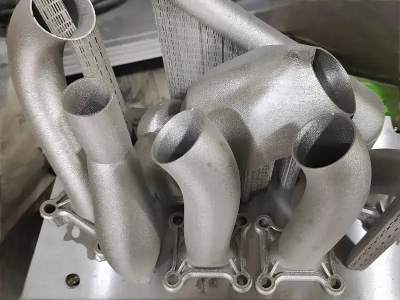
Metal additive manufacturing replaces the stack with one printed body. The waveguide channels, the mounting bosses, the feed network and the heat-sink features are built in the same operation. There is no flange between the radio and the radiating element, so there is no flange loss. That single change is the core of the pitch when Optisys introduces 3D printing of antennas to a new market.
The South Korean defense market matters here because the country has a dense aerospace and defense supply base plus a strong semiconductor and RF component ecosystem. Programs there tend to be integration-heavy: fewer platforms, more electronics per platform. When you are packing more RF channels into the same enclosure, part count and volume become the binding constraint, not raw gain.
The RF Physics That Make Printed Antennas Viable
A waveguide is a metal pipe sized so that a specific frequency band propagates inside it. The cutoff frequency depends on the internal width, not on how the outside of the pipe looks. That is the whole reason printing works. The process only has to control the internal channel geometry and the surface finish on the walls carrying current; the exterior can be any shape the packaging needs.
Skin depth is the second half of the argument. At 10 GHz in aluminum, current is concentrated in roughly the top 1 μm of the wall. The bulk of the metal is structure, not electrical function. A printed wall does not need to be thick to conduct, only to survive the mechanical and thermal loads of the application.
Surface roughness matters because it raises conductor loss. At Ka-band, a wall at Ra 1.6 μm will lose measurably more than the same wall at Ra 0.8 μm. This is where printed parts and machined parts get compared on equal terms: both need a controlled internal finish, and both need to prove it with a measurement rather than a visual check.
Which Geometries Belong in Metal Additive and Which Do Not
Printing wins when the part is topologically complex and low in count. An array that has to fit a curved radome, a feed network with dozens of splits, internal cooling channels running beside the RF path, or a lattice that removes mass without removing stiffness. Those are shapes a 5-axis mill cannot reach and a machinist cannot assemble economically.
Printing loses when the part is simple and the tolerance is tight. A straight waveguide run, a flat plate with a pattern of holes, a mounting bracket: these come off a mill faster, cheaper and closer to nominal. There is no reason to print a part that is already a straightforward 3-axis job.
There is also a size boundary. Printed RF housings are typically built inside a machine envelope measured in hundreds of millimeters, and the thermal distortion during the build grows with that envelope. When a single monolithic section is longer than the build allows, the design has to be split, and every split brings back the interface loss the printing was supposed to remove.
From RF Model to Finished Aperture: The Process Chain
The chain starts with the electromagnetic model, not the CAD model. The RF engineer sets the channel dimensions, the wall thickness and the transition geometry. The mechanical engineer then has to add everything the model does not care about: build supports, drain paths for un-melted powder, and a mounting interface that will survive vibration.
Powder removal is where printed RF parts quietly fail. A channel that looks clear on the screen may trap powder around a bend. If the trapped material stays in the part, it changes the effective dielectric constant inside the guide and shifts the response. The design has to include escape paths, and the shop has to verify them, usually with flow or borescope checks.
Post-processing decides whether the part meets the model. Internal surfaces that carry current get a controlled finish. Mating faces get machined flat, because a printed face is not a sealing face. Interfaces and threaded features are cut after the build, so the printed body is a near-net blank and the critical datums are established by machining.
- 1Design for drainageGive every internal channel an escape path for un-melted powder.
- 2Machine the interfacesFlanges, threads and sealing faces are cut after the build, not printed.
- 3Measure the wallsInternal roughness is a loss contributor and needs a number, not an opinion.
SWaP-C Gains and the Costs They Come With
SWaP-C stands for size, weight, power and cost. Printed RF front ends attack all four at once: fewer parts means less volume, less mass, fewer connectors to power and fewer assemblies to document. On a platform where every kilogram is budgeted, that is the argument that gets a design reviewed.
The counterweight is qualification. A printed RF part has process variables a machined part does not: build orientation, layer thickness, powder batch, heat treatment, and the surface state inside channels that are hard to inspect. Getting a part through vibration, thermal cycling and EMI testing takes a qualification plan, not just a good first article.
Cost also flips with volume. For one or two units, printing is often the only way to get the geometry at all. As volume climbs, the per-part cost of machining drops while the per-part cost of printing stays tied to build time. Around the low hundreds of units, the two curves usually cross and the decision changes.
Where CNC Machining Still Fits in an RF Program
Most printed RF assemblies still need machined parts. The housing that the printed aperture bolts into, the backing plate, the bracket that ties the assembly to the airframe, the connector bodies: those are conventional machining work and they carry the tight tolerances.
At GreatLight we hold ±0.005 mm (±0.0002 in) on critical features and finish internal bores to Ra 0.8–1.6 μm, with fine finishes down to Ra 0.2–0.8 μm when the RF path calls for it. Aluminum 6061-T6, 7075 and 2024 cover most waveguide and housing work; 17-4PH and Inconel come up when the part also has to survive heat or corrosion.
The practical split is simple. Print the geometry that cannot be machined. Machine the surfaces that have to be exact. A program that treats the two as competitors usually pays more than one that treats them as two steps in the same process.
Metal Additive vs CNC Machining for RF Parts
Use this to pick a route before you commit to a design review.
| Criterion | Metal additive | CNC machining | Best fit |
|---|---|---|---|
| Part count | One monolithic body | Multiple bolted parts | Additive when joints cost loss |
| Internal channels | Complex, curved, branching | Straight, reachable by tool | Additive for feed networks |
| Tolerance | Near-net, machined after | ±0.005 mm on critical faces | Machining for datums and flanges |
| Internal finish | Controlled but hard to inspect | Ra 0.8–1.6 μm repeatable | Machining for tight RF walls |
| Volume | Cost tied to build time | Cost falls with quantity | Machining above a few hundred units |
| Qualification | New process variables | Mature, documented | Machining for proven programs |
| Mass | Lattice and hollow features | Limited by tool access | Additive when weight drives design |
The Verdict
If the part is one complex RF body with internal channels and low volume, print it. If it is a simple geometry, a tight sealing face, or a run above a few hundred units, machine it. Most real programs need both, and the interface between them is where the work is.
Questions Engineers Ask Next
Can a printed waveguide hold tolerance without post-machining?
Not on the features that matter. The build gives you a near-net body, and the printed face carries a roughness and flatness that no sealing or mating interface should accept.
Plan for a machining step on flanges, threads and any face that sets a datum. The printed body supplies the complex internal geometry; the mill supplies the reference surfaces.
How do we inspect internal channels we cannot see?
Borescope and flow checks are the usual first pass. If the channel geometry is critical to the RF response, a witness coupon built in the same orientation gives you a cross-section to measure.
For production, the inspection plan has to be defined before the first build, not after. Reports on request are standard practice for us.
Does surface roughness inside the channel really change performance?
Yes, and it scales with frequency. At X-band the effect is modest; at Ka-band the conductor loss from a rough wall is a real line item in the budget.
Specify the internal finish as a number and say how it will be verified. A visual check is not a finish specification.
What aluminum grades work for RF housings?
6061-T6 is the default for housings and waveguide bodies: good machinability, stable, weldable. 7075 and 2024 come in when strength-to-weight drives the design.
For printed bodies, the alloy and heat treatment affect conductivity and dimensional stability, so the choice is a process decision, not just a material decision.
How do we split the work between a printer and a machine shop?
Send the RF model and the mechanical envelope together. We review what can be printed, what has to be machined, and where the interface should sit so the loss budget is not spent on a joint.
Quotation and DFM analysis come back within 12 hours, and production can start within 24 hours of approval.
Can you work under NDA on defense-adjacent programs?
Yes. Uploads are secure and confidential, and an NDA is available on request. We hold ISO 9001:2015, IATF 16949:2016, ISO 13485:2016 and ISO 27001:2022.
Every part is 100% inspected before shipment, with raw material check, in-process monitoring and final inspection.
Send the RF Model, Get a Machining Plan
Upload the RF body and the housing together. We will tell you which features to print, which to machine, and what the interface should look like.
12-hour quote±0.005 mm100% inspectionNo minimum order quantity
More process notes from the shop
We publish setup notes, tooling trials and inspection data from the factory floor.