Unleashing the Power of Kicad: A Comprehensive Guide to Designing Electronic Diagrams and Printed Circuits
In an increasingly complex and interconnected world, the need for efficient and effective design tools has become a critical component of modern electronics. Kicad, a powerful Windows application, has risen to the challenge by providing a user-friendly platform for designing electronic diagrams and printed circuits. In this blog post, we’ll delve into the features and capabilities of Kicad, exploring its capabilities for designing and debugging printed circuits, and getting the most out of this innovative tool.
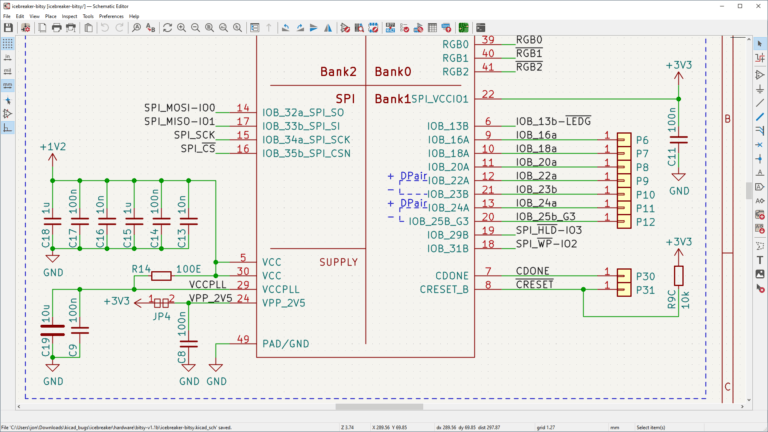
Schematic Design and Editing: The Fundamentals
At its core, Kicad’s schematic editor is designed to facilitate the creation of electronic diagrams, allowing users to configure page parameters, perform basic editing operations, and draw wires and buses with ease. This intuitive interface ensures that even novice designers can quickly get started with creating a new project. Key features include:
- Local and global labeling: Assign standardized labels to components, making it easier to identify and manage complex circuits.
- Connection points: Establish connections between components, streamlining the design process and reducing errors.
- Error detection and warning messages: The software’s built-in validation system detects and alerts users to potential issues, reducing the likelihood of costly rework.
PCB Design and Visualization
Kicad’s PCB editor takes things to the next level, offering a range of advanced features for designing and visualizing printed circuits. Key capabilities include:
- Macro support: Utilize pre-defined actions and shortcuts to streamline your workflow, reducing repetition and increasing productivity.
- Integrated PCB viewer: Visualize and inspect your designs, ensuring accurate and efficient execution.
- 3D visualization: Explore your designs in 3D, providing a more immersive and intuitive understanding of your printed circuit boards.
Design Automation and Customization
Kicad also offers a range of features designed to streamline the design process, including:
- Design rule management: Establish and enforce design standards, ensuring consistent and high-quality results.
- Layer management: Organize and manage layers, making it easier to focus on specific components and sections.
- Text and polygon integration: Easily add text and polygons to your design, enhancing its clarity and functionality.
- Export options: Export your designs in various formats, including GERBER, CAD, and WRL.
Beyond the Basics: Advanced Features and Capabilities
Kicad’s feature set extends far beyond the basics, offering a range of advanced tools and capabilities for the more experienced designer. Some standout features include:
- Footprint library integration: Draw upon an extensive library of pre-defined component footprints, speeding up the design process.
- 3D modeling: Create complex 3D models, allowing you to visualize and explore your designs from multiple angles.
- Gerber file analysis: Analyze and edit GERBER files, providing a deeper understanding of circuitry and functionality.
- PCB calculator: Automate calculations and conversions, saving time and reducing the risk of errors.
Conclusion
Kicad has established itself as a leading tool for designing electronic diagrams and printed circuits, offering a range of features and capabilities designed to meet the needs of both novice and experienced designers. With its intuitive interface, advanced design tools, and strong support for design automation, Kicad is an essential resource for anyone working in the fields of electronics and PCB design. Whether you’re looking to create complex circuit boards or simply need to streamline your design process, Kicad is the perfect tool to get you there.