Unlocking semiconductor excellence: The key role of CNC machining
The semiconductor industry is booming in innovation, breaking the boundaries between miniaturization and performance. Behind each cutting-edge chip is a complex ecosystem of manufacturing equipment (from lithography machines to wafer processing personnel), in units of unparalleled precision. This is CNC machining Appearing as a silent power, transforming complex design into reality. exist GreatWe use advanced five-axis CNC technology to solve the toughest manufacturing challenges in the semiconductor sector and drive innovation at a microscopic scale.
Semiconductor manufacturing: Accuracy is not negotiable
Semiconductor manufacturing equipment operates in extremely precise fields:
- Tolerance threshold: The components must be in tolerances up to ±0.001 mm, equal to 1/100 of human hair.
- Complex geometric shapes: The radiator, plasma chamber and wafer stages require free form surfaces, non-orthogonal angles and low-light smoothness.
- Material requirements: The parts must resist corrosion, thermal stress and pollution and need to have foreign alloys such as titanium, inconel or alumina ceramics.
Traditional processing is insufficient here. Even slight deviations can lead to particle contamination, thermal warping or electrical interference, and damage to the yield rate.
Five-axis CNC: Accuracy accelerator for semiconductor sector
Unlike a 3-axis machine, the five-axis CNC system dynamically rotates tools and workpieces on multiple planes in a single setup. This can:
- Uncompromising accuracy: The contour capability eliminates repositioning errors, thus maintaining the integrity of the curved geometry.
- Perfect surface: Continuous tools are involved in ensuring a surface finish of RA <0.4μm, which is critical to vacuum seal integrity and particle control.
- Improved efficiency: Complex parts (such as turbomolecular pump rotors) are processed 60%, faster than the multi-step process.
In Greatlight, our DMG Mori and Haas five-axis center Integrate AI-driven error compensation, vibration damping and process metrology to achieve "First right" Quality of key components:
- Etch nozzles with micro-cold channel
- EUV lithography frame
- CVD reactor hood
GRESTHILE: Your partner in semiconductor accuracy
We blend cutting-edge technologies with industry-specific expertise to deliver unparalleled manufacturing solutions.
1. Advanced five-axis mastery
Our facility has 12 multi-piece five-axis machining cells with adaptive tool control, making:
- Microarrangement function: Tools that drop to 0.1 mm for complex functions.
- Thermal stability: Climate-controlled environment (±0.5°C) prevents material drift.
- On-board detection: Real-time quality verification reduces inspection time by 80%.
2. Material versatility without compromise
From aluminum alloy for light robotics to Molybdenum with thermal uniformityWe have mastered more than 50 certification materials. Professional processes include:
- Non-magnetic processing: Cobalt chromium is used as the MRI-sensitive ingredient.
- Ceramic grinding: The alumina and zirconia fractions are <1 μm concentric.
3. One-stop completion and certification
We bridge machining, ready for the end use of integrated services:
- Super Clean: Level 10 clean room particle removal.
- Professional paint: Corrosion resistance of PVD, electronic coating and anodizing.
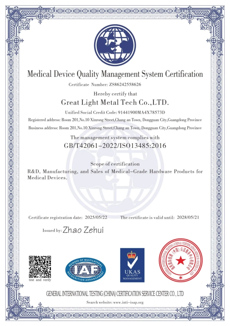
- Compliance Documents: Traceability and PPAP verification for ISO 9001 certification.
4. Advantages of fast market access
Using digital threads from CAD to QC, we 5~7 days and large batch processing 15 dayswith strict DFM feedback to avoid redesign loops.
Conclusion: Design precision for tomorrow’s semiconductors
In a nano-definition successful industry, Greatlight’s five-axis CNC solutions enhance innovation capabilities. We transform complex semiconductor designs into flawless, production-ready components that accelerate your R&D cycle while ensuring large-scale reliability. From prototyping to high volume manufacturing, our technical proficiency, material expertise and end-to-end service convergence makes us a Excellent unrivalled partner.
Are you ready to design breakthrough semiconductor devices?
➡️Customize your precision parts now
FAQ: CNC machining for semiconductor applications
Q1: Can you process parts for ultra-high vacuum (UHV) environments?
Absolutely. We specialize in UHV-compatible components, utilizing vacuum rating materials such as 316L stainless steel or aluminum alloy, paired with electropolished and non-combustible coatings to prevent shedding or particles from falling off.
Q2: How to ensure EMI/RFI shielding in semiconductor tools?
We integrate conductive plating (e.g., nickel copper) during the installation functions of post-processing and design isolation to prevent electromagnetic interference and verified by third-party testing.
Q3: What tolerances can wafer processing robots achieve?
We usually use machine CMM and iterative compensation algorithms to routinely maintain position accuracy of ±0.005 mm and concentricity of robot arms.
Question 4: Do you support low-capacity prototyping for R&D projects?
Yes. Our agile workflows provide functional prototypes in just 72 hours and provide manufacturability feedback to optimize part performance and cost.
Question 5: How to reduce the risk of pollution in five-axis processing?
Single-piece setting machining minimizes processing and eliminates alignment debris. In conjunction with the packaging of the clean room, we ensure that the components are in compliance with ISO Level 5 standards upon delivery.
Question 6: Can you create conformal cooling channels in diffusion furnace parts?
Our five-axis system milled complex internal channels narrow to 0.8 mm and have smooth bending to optimize thermal management and validated by flow simulation and stress testing.